How can a NOT gate function with a misplaced resistor?

  • Thread starter wannab
  • Start date
  • Tags
    Gate Work
In summary: Transistors are generally one of the tougher things to master in electronics. (for normal people anyways) The reason why your circuit doesn't work is because current always splits up and takes all paths to ground. A resistor at the output ensures that the current will flow to ground.
  • #1
wannab
32
1
I found an image on google that I recognised to be an almost functioning NOT gate:
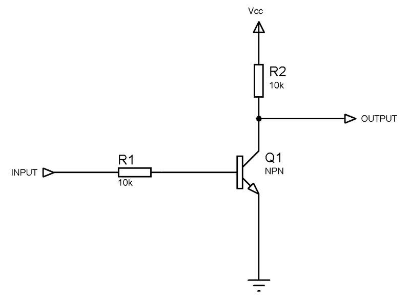
not.bmp.jpg


But I felt the resistor was misplaced so I changed it to put it here:

B5xVneu.jpg


Who is correct and why? The only way I can see the first image functioning as a NOT gate is if the transistor somehow has a negative resistance when its base is active, is this the case?
 
Engineering news on Phys.org
  • #2
Your diagram is wrong. The first diagram is correct.
Why you think that the first diagram is wrong ?
 
  • #3
The first diagram is a NOT gate.

The second diagram represents a blown transistor waiting to happen.
 
  • #4
The first diagram is a-NOT-Gate.

The second diagram is NOT-a-Gate.

:smile:
 
  • #5
Jony130 said:
Your diagram is wrong. The first diagram is correct.
Why you think that the first diagram is wrong ?
Because the electricity has no incentive to flow to ground, it will always take the shortest route which will either be to the output or the ground depending on the resistances and lengths of the wires. By putting a resistor at the output I'm ensuring that the current will flow to ground once the base of the transistor is active.
 
  • #6
So confused.
 
  • #7
In this circuit the BJT work in cut-off region (no base current flow).
Or in saturation, (base-emitter current is flowing).
So if transistor is full on (saturated), then he act just like a shorted switch.
Short collector to GND. Or in general shots the collector to emitter.
52_1250869699_thumb.png
 
  • #8
wannab said:
Because the electricity has no incentive to flow to ground, it will always take the shortest route which will either be to the output or the ground depending on the resistances and lengths of the wires. By putting a resistor at the output I'm ensuring that the current will flow to ground once the base of the transistor is active.

First of all, in this circuit, there is nothing connected to the output (it is open) so current can't go that way anyway. But even if there were a load connected to the output, you are suffering from a common misconception. Current always splits up and takes all paths to ground. The amount of current on each path is inversely proportional to the resistance of that path. What we mean when we say that "current takes the path of least resistance" is that, if there is one path whose resistance is drastically lower than any of the others, then the vast majority of the current will take that path and not the others.

Second, the reason why your circuit doesn't work is as follows. In this regime, the transistor acts somewhat like a switch. If the base voltage is low, there will be no connection between the collector and emitter: the transistor does not conduct. If the base voltage is high, the transistor conducts between collector and emitter. It acts kind of like a switch. In fact, to see what's going on conceptually, you could just replace the BJT with a switch that is closed when Vin is high, and open when Vin is low, So, in your version of the circuit, where you have no resistor between Vcc and the collector, when the transistor conducts, it's like the switch closes, connecting Vcc directly to ground through a negligible resistance. You've shorted your power supply. So, a tremendous amount of current will be drawn. Can you see why this is a tremendously bad idea, as phinds already alluded to? EDIT: Also at that point, your resistor R2 actually does nothing at all, because it has literally been shorted out of the circuit.
 
  • #9
wannab said:
So confused.

Not to worry. Transistors are generally one of the tougher things to master in electronics. (for normal people anyways)
 
  • #10
cepheid said:
First of all, in this circuit, there is nothing connected to the output (it is open) so current can't go that way anyway. But even if there were a load connected to the output, you are suffering from a common misconception. Current always splits up and takes all paths to ground. The amount of current on each path is inversely proportional to the resistance of that path. What we mean when we say that "current takes the path of least resistance" is that, if there is one path whose resistance is drastically lower than any of the others, then the vast majority of the current will take that path and not the others.
If that's true then surely when the transistor is active the current would split, some going to output and some going to ground? That's not what is required though, what's required is absolutely no current going to output and all of it going to ground.

Surely we need a resistor at the output to encourage more electricity to go to ground when the transistor is active?
 
  • #11
Also what's the difference between an AND gate and a transistor? To me they appear to do the same thing. This might be the source of my confusion.
 
  • #12
wannab said:
If that's true then surely when the transistor is active the current would split, some going to output and some going to ground? That's not what is required though, what's required is absolutely no current going to output and all of it going to ground.

No, what's required is that the voltage between the output and ground is below a given threshold. And that will be the case if the components are chosen correctly. No matter what resistance is connected to the output. There can be some current flowing through the output even if it's in the low state as long as the voltage is low enough.
 

1. What is a NOT gate and how does it work?

A NOT gate, also known as an inverter, is a logic gate that has one input and one output. It performs the logical operation of negation, meaning it will output the opposite of the input. For example, if the input is 0, the output will be 1, and vice versa.

2. How is a NOT gate different from other logic gates?

A NOT gate is different from other logic gates because it only has one input and one output, while other gates such as AND and OR gates have multiple inputs and a single output. Additionally, a NOT gate only performs a negation operation, while other gates perform different logical operations.

3. Can a NOT gate be used in combination with other logic gates?

Yes, a NOT gate can be used in combination with other logic gates to create more complex logic circuits. It is often used in combination with other gates to invert the output of a circuit or to create a specific logic function.

4. How is a NOT gate implemented in electronic circuits?

A NOT gate can be implemented using various electronic components such as transistors, diodes, and resistors. The most common implementation is using a transistor as a switch, where the input is connected to the base of the transistor and the output is taken from the collector. When the input is high, the transistor is turned off, and the output is low. When the input is low, the transistor is turned on, and the output is high.

5. What are some real-life applications of NOT gates?

NOT gates have many applications in digital electronics, such as in logic gates, flip-flops, and memory units. They are also used in microcontrollers, computer processors, and other digital circuits. In real-life, NOT gates are used in various electronic devices, such as calculators, cell phones, and computers.

Similar threads

Replies
80
Views
3K
Replies
4
Views
2K
  • Introductory Physics Homework Help
2
Replies
56
Views
2K
Replies
68
Views
3K
  • Electrical Engineering
Replies
3
Views
3K
Replies
1
Views
780
  • Electrical Engineering
Replies
12
Views
3K
Replies
3
Views
1K
  • Introductory Physics Homework Help
Replies
9
Views
579
  • Electrical Engineering
Replies
6
Views
939
Back
Top