Transistor not gate function

In summary: The circuit works because when the input goes low, current is steered to the base of Q2, causing it to saturate. When the input goes high, current is not steered and the output stays at 5 volts.The circuit works because when the input goes low, current is steered to the base of Q2, causing it to saturate. When the input goes high, current is not steered and the output stays at 5 volts.
  • #1
tmiddlet
26
0
Transistor "not gate" function

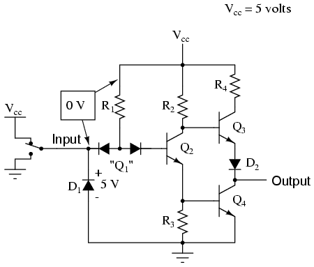
I've been trying to understand the following circuit:
04075.png


I'm new to circuitry and electrical engineering, so I've had some trouble understanding the function of transistor Q3 and diode D2, I believe the circuit should function without them. If anybody could describe to me their function, that would be great, I under stand the rest.

Thanks!
 
Engineering news on Phys.org
  • #2


I don't understand the 0 V arrow pointing to Vcc as when the switch is grounded, the input would be 0 V but not Vcc which is 5 volts.

Anyway, when the switch/input is at 5volts, Q2 will saturate and its collector voltage will be low causing Q3 to not saturate also the emitter voltage of Q2 will be high causing Q4 to saturate, so the output would be low (saturation collector to emitter= ~0.2V). Hence the inverter; input high=5V, output low=0.2V.

Now when the switch/input is at 0volts, Q2 will not saturate and its collector voltage will be high causing Q3 to saturate also the emitter voltage of Q2 will be low causing Q4 to not saturate, so the output will be high (Vcc -saturation collector to emitter=~4.8V). Hence the inverter; input low=0V, output high=4.8V.

And I believe the diode, D2 is there to prevent whatever is connected to the output not to back feed current into your circuit. But I may be wrong on this point.

Hope this helps
 
  • #3


The 0 volt arrows just indicate a zero volt difference, so the diode doesn't activate.

Because Q3 and D2 don't seem to significantly change the output voltage, I think you're probably right, they're probably protecting the circuit from back feed current.

They were confusing because they don't seem to affect the behavior of the circuit significantly.
 
  • #4


tmiddlet said:
The 0 volt arrows just indicate a zero volt difference, so the diode doesn't activate.

Because Q3 and D2 don't seem to significantly change the output voltage, I think you're probably right, they're probably protecting the circuit from back feed current.

They were confusing because they don't seem to affect the behavior of the circuit significantly.

Well here's an explanation of what's happening and why the transistors of this circuit

319px-7400_Circuit.svg.png


To solve the problem with the high output resistance of the simple output stage the second schematic adds to this a "totem-pole" ("push–pull") output. It consists of the two n-p-n transistors V3 and V4, the "lifting" diode V5 and the current-limiting resistor R3 (see the figure on the right). It is driven by applying the same current steering idea.[12]

When V2 is "off", V4 is "off" as well and V3 operates in active region as a voltage follower producing high output voltage (logical "1"). When V2 is "on", it activates V4, driving low voltage (logical "0") to the output. V2 and V4 collector–emitter junctions connect V4 base–emitter junction in parallel to the series-connected V3 base–emitter and V5 anode–cathode junctions. V3 base current is deprived; the transistor turns "off" and it does not impact on the output. In the middle of the transition, the resistor R3 limits the current flowing directly through the series connected transistor V3, diode V5 and transistor V4 that all are conducting. It also limits the output current in the case of output logical "1" and short connection to the ground. The strength of the gate may be increased without proportionally affecting the power consumption by removing the pull-up and pull-down resistors from the output stage.[16][17]

http://en.wikipedia.org/wiki/Transistor–transistor_logic#TTL_with_a_.22totem-pole.22_output_stage"
 
Last edited by a moderator:
  • #5


Thanks for the link, that was a good description, the only part I don't understand is:
The resistor R3 does not increase the output resistance since it is connected in the V3 collector and its influence is compensated by the negative feedback

I don't see why R3 doesn't increase the output resistance
 
  • #6


tmiddlet said:
Thanks for the link, that was a good description, the only part I don't understand is:


I don't see why R3 doesn't increase the output resistance

...transistor V3 operating in active region as a voltage follower...

The key words here are "voltage follower".

Other unity gain buffer amplifiers include the bipolar junction transistor in common-collector configuration (called an emitter follower because the emitter voltage follows the base voltage, or a voltage follower because the output voltage follows the input voltage)...

Bold emphasis by me.

http://en.wikipedia.org/wiki/Voltage_follower#Single-transistor_circuits"
 
Last edited by a moderator:
  • #7


It's been a while since I was doing this stuff but I can't see why is there no 'pull down' resistor somewhere in the base circuit of Q2?
Any ideas?
 
  • #8


sophiecentaur said:
It's been a while since I was doing this stuff but I can't see why is there no 'pull down' resistor somewhere in the base circuit of Q2?
Any ideas?
In the circuit note that "Q1" is a transistor like in this circuit,

04073.png


It's from this site where the OP, I'm guessing, got the circuit.

http://www.allaboutcircuits.com/vol_4/chpt_3/2.html"
Here, the base charge of Q2 gets dissipated by the collector of Q1, when the input goes low, causing Q2 to cut-off. Then when the input goes high, current is steered to the base of Q2, causing it to saturate. So there is no need for a pull-down resistor.
 
Last edited by a moderator:

What is a transistor?

A transistor is a semiconductor device that can amplify or switch electronic signals. It consists of three layers of a material, such as silicon, with impurities added to create a positive and negative layer. By applying a small current to one layer, the transistor can control a larger current flowing through the other two layers.

What is a not gate?

A not gate, also known as an inverter, is a logic gate that takes in a single input and produces the opposite output. It is represented by the symbol "NOT" and has a truth table that shows that for every input value of 0, the output is 1, and for every input value of 1, the output is 0.

How does a transistor work as a not gate?

A transistor can function as a not gate by using the input signal to control the flow of current through the other two layers. When the input is low (0), the transistor allows current to flow through, resulting in a high output (1). When the input is high (1), the transistor blocks the flow of current, resulting in a low output (0).

What are the applications of a not gate?

A not gate has many applications in digital circuits, such as inverting signals, creating oscillators, and performing logical operations. It is also used in memory circuits, microprocessors, and computer systems.

What are the advantages of using a transistor as a not gate?

Transistors are small, fast, and reliable, making them ideal for use in not gates. They also consume less power, generate less heat, and are less expensive compared to other electronic components, making them a cost-effective option for implementing logic functions.

Similar threads

Replies
68
Views
3K
  • Electrical Engineering
Replies
5
Views
1K
Replies
8
Views
867
  • Electrical Engineering
Replies
7
Views
1K
  • DIY Projects
Replies
2
Views
4K
  • Electrical Engineering
Replies
2
Views
1K
  • Electrical Engineering
Replies
14
Views
2K
Replies
1
Views
780
  • Electrical Engineering
Replies
23
Views
4K
Replies
6
Views
2K
Back
Top