Cascode Amp Questions: Exploring C1 and C2

  • Thread starter perplexabot
  • Start date
  • Tags
    Amp
In summary, the conversation is about a cascode RF amplifier and the role of the capacitors C1 and C2 in the circuit. The expert summarizer explains that the capacitors play a crucial role in providing a stable DC bias and preventing signal distortion. They also mention the purpose of the other components in the circuit, such as L1 and R2, in isolating the RF signal and setting the gain. The conversation also touches on the biasing of the gate and the role of the depletion mode FET in regulating the cascode chain bias current.
  • #1
perplexabot
Gold Member
329
5
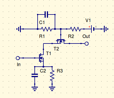
Hello all. I have been looking into RF amps. I have come across the following cascode amp (from ARRL handbook 2014, p 12.10, FIG. 12.11. Thanks to Baluncore for the great reference). Here is a simplified version made with Qucs:
cascode.png


My questions are regarding the capacitors, C1 and C2. Why are they there?

I know that if we were to have only a common source (CS) amplifier the bypass capacitor C2 will provide a larger gain for the small signal required. But this is not the case here, if I am not mistaken, in a cascode configuration, the CS phase does not provide amplification, it provides high input impedance, right? If yes, then why do we care about the small signal gain at that point. Is it not the common gate stage that provides amplification?

I have no idea why C1 is there! I know R1 and R2 set up the Voltage bias at T2, I also know that for small signal, the gate will look like a ground, what is the point of C1?

Thank you.
 
Engineering news on Phys.org
  • #2
It is not "common source" if the source is not "common" or at ground to both input and output, so the source is connected to ground via that capacitor. Similarly, with the biasing at gate of T2 it can't be common gate unless the gate is grounded at signal frequencies. The gate won't 'look like a ground' if there are resistors in the way.

Edit: you are probably going to say because the gate draws no current, what does it matter if there is series resistance. I'd think you don't want any extraneous signal to be induced on the wiring to the gate, and any internal leakage signal making its way to the gate should be shunted to ground via very low impedance so it can't create its own gate voltage.
 
Last edited:
  • Like
Likes 1 person
  • #3
NascentOxygen said:
It is not "common source" if the source is not "common" or at ground to both input and output, so the source is connected to ground via that capacitor. Similarly, with the biasing at gate of T2 it can't be common gate unless the gate is grounded at signal frequencies. The gate won't 'look like a ground' if there are resistors in the way.

Amazing, that makes a lot of sense. Thank you so much.

Edit: Thanks for the "edit." I was not wondering about it but it helps that you mentioned it.
 
  • #4
Hey again. Sorry for resurrecting this thread but it isn't that old and I have a question pertaining to the same circuit. So after some simulations, I got the output to look like it should but I have two questions. Here is the circuit I used in LTSpice:
cascode-1.png


Q1] Why is it that J1 doesn't have to be biased? For a common source amplifier one would have to bias the gate appropriately to not have signal distortion. At first I tried having the signal ride on DC but had weird results (it would alter my input frequency!). Why is it that J1 does NOT have to be biased?

Q2] What is the job of L1 and R2? I know at DC L1 will seem to be a short, and it will not see R2. I also know at certain frequencies L1 will seem to be a very high impedance and only see R2. What is the point of this?

Thank you.
 
Last edited:
  • #5
You have two distinct paths. One is the DC bias, the other is the RF signal.
Those paths are separated by the L and C components.

J1 is a depletion mode FET. The gate is DC biassed to ground by R1.
The current bias is set by the negative gate voltage divided by the value of R5.
C1 gives the V3 input AC signal on the gate something solid for the source to work against by hiding the DC value of R1 behind the low impedance of C1 at RF.

I presume your RF output is appearing across R6.
L1 is an RF choke that isolates the RF output signal from the low impedance power supply bypass cap C5.
L1 also carries the DC bias current around R2 and so reduces the need for a higher supply voltage.
R2 sets, or limits, the output stage RF gain.
R2 also prevents self resonance of L1, RF chokes were once often wound on the resistors.
 
  • Like
Likes 1 person
  • #6
Baluncore said:
You have two distinct paths. One is the DC bias, the other is the RF signal.
Those paths are separated by the L and C components.

J1 is a depletion mode FET. The gate is DC biassed to ground by R1.
The current bias is set by the negative gate voltage divided by the value of R5.
C1 gives the V3 input AC signal on the gate something solid for the source to work against by hiding the DC value of R1 behind the low impedance of C1 at RF.

I presume your RF output is appearing across R6.
L1 is an RF choke that isolates the RF output signal from the low impedance power supply bypass cap C5.
L1 also carries the DC bias current around R2 and so reduces the need for a higher supply voltage.
R2 sets, or limits, the output stage RF gain.
R2 also prevents self resonance of L1, RF chokes were once often wound on the resistors.

Great information. Thank you for answering my question and more.

The only thing that I have a hard time understanding is when you say: "The current bias is set by the negative gate voltage divided by the value of R5."

Maybe if I work out the math of the circuit I will understand better what you meant... Thanks again for all the help.
 
  • #7
The Gate-Source voltage of an MPF102 is specified at VDS = 15 Vdc, ID = 0.2 mAdc as being between −0.5 and −7.5 Vdc.

The gate of the depletion mode FET is therefore more negative than the source, so a source resistor can make a very simple DC current regulator that sets the cascode chain bias current.

The gate-source voltage appears across R5 and sets the bias. Gain is then approximately R5 / R2.
 
  • #8
Baluncore said:
The Gate-Source voltage of an MPF102 is specified at VDS = 15 Vdc, ID = 0.2 mAdc as being between −0.5 and −7.5 Vdc.

The gate of the depletion mode FET is therefore more negative than the source, so a source resistor can make a very simple DC current regulator that sets the cascode chain bias current.

The gate-source voltage appears across R5 and sets the bias. Gain is then approximately R5 / R2.

Interesting, so if J2 is biased correctly it is seen as a short (a wire) looking into its source? Hence the gain of approximately R5/R2?
 
  • #9
Sorry, I got that wrong, twice. Without C1 the RF gain would be controlled by the R2 / R5 resistor ratio.
But with C1 present the RF gain is a function of the Drain current to Gate-Source voltage relationship, (Gm), and the value of R2.

J2 is a source follower, the gate is fixed so there is little voltage variation on the source.
That prevents voltage changes on the drain of J1.
So the “miller” capacitance between the gate and drain of J1 is not such a frequency limiting factor.

Cascode isolates the J1 gate input from the J2 drain output.
That is why the cascode arrangement is used. It works well at VHF and UHF.
 
  • #10
Baluncore said:
Sorry, I got that wrong, twice. Without C1 the RF gain would be controlled by the R2 / R5 resistor ratio.
But with C1 present the RF gain is a function of the Drain current to Gate-Source voltage relationship, (Gm), and the value of R2.

J2 is a source follower, the gate is fixed so there is little voltage variation on the source.
That prevents voltage changes on the drain of J1.
So the “miller” capacitance between the gate and drain of J1 is not such a frequency limiting factor.

Cascode isolates the J1 gate input from the J2 drain output.
That is why the cascode arrangement is used. It works well at VHF and UHF.

Thank you so much!
 

1. What is a cascode amplifier?

A cascode amplifier is a type of circuit that uses two transistors in a series configuration to amplify a signal. The input signal is applied to the first transistor, which then amplifies it and sends it to the second transistor for further amplification.

2. What is the purpose of C1 and C2 in a cascode amplifier?

C1 and C2 are capacitors that are used to stabilize the cascode amplifier, especially at high frequencies. C1 is typically used to bypass the input resistor and improve the amplifier's gain and bandwidth, while C2 is used to reduce the Miller effect and improve the amplifier's stability.

3. How do C1 and C2 affect the frequency response of a cascode amplifier?

C1 and C2 play a crucial role in shaping the frequency response of a cascode amplifier. C1 can improve the low-frequency response by bypassing the input resistor, while C2 can improve the high-frequency response by reducing the Miller effect. Both capacitors can also improve the overall stability of the amplifier.

4. What are the typical values for C1 and C2 in a cascode amplifier?

The values of C1 and C2 can vary depending on the specific design and application of the cascode amplifier. However, in general, C1 is typically in the range of a few picofarads to a few hundred picofarads, while C2 is usually in the range of a few nanofarads to a few hundred nanofarads.

5. How do I determine the optimal values for C1 and C2 in a cascode amplifier?

The optimal values for C1 and C2 can be determined through simulation or experimentation. Factors to consider include the desired frequency response, stability, and overall performance of the amplifier. It is also important to consider the parasitic capacitances of the transistors and the layout of the circuit when selecting the values for C1 and C2.

Similar threads

  • Electrical Engineering
Replies
3
Views
797
  • Electrical Engineering
Replies
14
Views
4K
  • Electrical Engineering
Replies
32
Views
5K
  • Electrical Engineering
Replies
4
Views
5K
  • Electrical Engineering
Replies
8
Views
2K
  • Electrical Engineering
Replies
7
Views
1K
Replies
14
Views
2K
  • Engineering and Comp Sci Homework Help
Replies
22
Views
3K
  • Electrical Engineering
Replies
6
Views
2K
Replies
5
Views
2K
Back
Top