P-n junction & transistors: depletion zone

In summary: I'm not sure what you're looking for specifically, but I can tell you that the depletion zone for a p-n junction gets wider when the p side is more positive, and narrower when the n side is more positive. The depletion zone for a transistor is different because there is no battery connected. When the transistor is "on", there is no gap electrons must be shoved across, so there is no extra voltage necessary to push electrons through.Thanks again!
  • #1
sparkle123
175
0
For p-n junctions (connected as a junction rectifier), the forward-bias connection (battery's positive terminal connected at the p side) results in a narrowed depletion zone, because: the p side becomes more positive and the n side becomes more negative, thus decreasing the height of the potential barrier
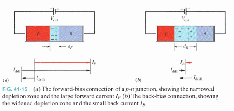
9685a15c.png


So why in transistors, does the negative gate which repel electrons from the n channel down into the substrate widen the depletion zone, instead of narrowing it, as in p-n junctions?

692dd7df.png


Thank you very much! I hope my question is adequately clear :)
 
Last edited:
Physics news on Phys.org
  • #2
The conduction mechanism is different for the two devices. For the diode, obviously there is still a gap of non-conductive material, its just that that gap is notably thinner when the diode is forward-biased. But there is still a gap and that's why you'll need at least about .6V (for silicon, anyway) of forward voltage to get the electrons to jump across that gap. The FET does not suffer from this because its conduction mechanism is different. When the FET is 'on', there is no gap electrons must be shoved across, so there is no extra voltage necessary to push electrons through.
 
  • #3
Thanks fleem! :)
can you please explain why the depletion zone is widened in the FET case?
 
  • #4
The diagram doesn't show it, but the depletion region in the FET's n-channel is lacking in electrons because the nearby P substrate stole them. When a field is applied, it helps the P-substrate steal more electrons deeper into the n-channel, so the region of the n-channel that contains carriers (electrons) is narrower. In the diode diagram you can see how the P steals some electrons from the nearby N material.
 
  • #5
Thanks again!
I'm still a little confused why the FET depletion region becomes wider when P steals electrons, but the diode depletion region becomes narrower when P steals electrons?
 
  • #6
A depletion region is a region in which carriers have been removed so that there is less conductivity. For both the FET and the diode, the depletion region becomes wider when the the P steals electrons (and N steals holes).
 
  • #7
but according to the first diagram, the depletion region becomes narrower when the P steals electrons in the diode?
 
  • #8
The depletion region is the light-blue area down the center of the crystal between the N and P. the diagrams show charges in that region (pluses and minuses). The region is wider on the right diagram because there the P material has more electrons and N has more holes. On the left, the depletion region is thinner because the P has fewer electrons and the N has fewer holes.
 
  • #9
thanks again! but-
in the left diagram, the negative terminal is connected to the N material and depletion zone is NARROWER
in the MOSFET the negative terminal is connected to the N material and depletion zone is WIDER
 
  • #10
Ah I think I see the confusion now. Maybe your question can be reworded: Why does the P region steal MORE electrons from the N region when the P region has a negative charge (and vice versa for the N region)--it seems its negative charge would cause it to steal fewer electrons? The answer is, I think, that I shouldn't have stressed so much that the P "steals electrons" from the N. It does, and it is especially apparent when there is no battery connected, but the battery (when connected as shown in the right diagram) steals even more carriers from the both the P and N. The negative terminal on the battery shoves electrons into the P, filling the holes and thus removing those carriers, and vice versa for the N region.
 
  • #11
haha this is confusing...thanks for you help!
 
  • #12
Hi everyone,

I was wondering where i could find information relating to depletion zone thickness for silicon p-n junctions. Am doing it for a project on solar cells.

Also, what actually happens to the thickness of the depletion zone when the solar cells are active in closed or open circuit condition,would it be different?

btw would anyone know where to find values for diffusion lengths also?

Thanks lots
 

1. What is a P-n junction?

A P-n junction is a type of semiconductor junction formed by combining a p-type semiconductor (with positively charged carriers) and an n-type semiconductor (with negatively charged carriers). This results in a depletion zone at the junction, creating a barrier for the flow of current.

2. How does the depletion zone affect the behavior of a transistor?

The depletion zone acts as a barrier for the flow of current, which makes it an important part of a transistor's functioning. By applying a small voltage to the depletion zone, the barrier can be reduced or eliminated, allowing for the flow of current. This allows transistors to be used as switches or amplifiers in electronic circuits.

3. What is the role of impurities in creating the depletion zone?

Impurities, also known as dopants, are intentionally added to the semiconductor materials to create the p-type and n-type regions. These impurities have an uneven distribution of electrons, which creates a difference in charge within the material and results in the formation of the depletion zone at the junction.

4. How does the size of the depletion zone affect the performance of a transistor?

The size of the depletion zone can be controlled by the amount of voltage applied to it. A larger depletion zone allows for a higher resistance and a smaller flow of current, while a smaller depletion zone allows for a lower resistance and a larger flow of current. This control over the depletion zone allows for the precise functioning of transistors in electronic circuits.

5. Can the depletion zone be reversed?

Yes, the depletion zone can be reversed by applying a reverse voltage to the junction. This will cause the depletion zone to widen, further restricting the flow of current. This property is used in diodes, which are a type of semiconductor device that only allows current to flow in one direction.

Similar threads

  • Introductory Physics Homework Help
Replies
18
Views
2K
  • Introductory Physics Homework Help
Replies
4
Views
3K
Replies
2
Views
2K
  • Engineering and Comp Sci Homework Help
Replies
1
Views
798
Replies
3
Views
741
  • Electrical Engineering
Replies
3
Views
2K
  • Introductory Physics Homework Help
Replies
4
Views
1K
Replies
30
Views
5K
Replies
5
Views
2K
  • Electrical Engineering
Replies
8
Views
15K
Back
Top