Confused about transistor saturation region

In summary, the saturation region in a transistor is where the collector current is no longer linearly proportional to the base current and is instead determined by the collector voltage and resistance. This is referred to as saturation because the transistor is "bottoming out" and can no longer be turned on any further. The active region, where the base has control of the collector current, may have a higher collector current than the saturation region, but it is the point where the transistor is on the verge of saturation. Additionally, the transistor has a "upside-down" configuration in the saturation region due to the forward biased b-c junction, resulting in both base and collector currents.
  • #1
Nat3
69
0
Confused about transistor "saturation" region

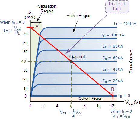
I don't understand why the saturation region is called the saturation region. Take a look at the graph below:
tran11.gif


According to that graph, the "saturation" region is where the current changes most rapidly, which is the exact opposite of the definition of saturation! It seems like the active region should be called the saturation region, right?

Also, I've read that the maximum collector/emitter current occurs when the transistor is in the saturation region, but it's clear from the graph that the collector current is higher in the active region than in the saturation region, right?

I'm confused :confused:
 
Engineering news on Phys.org
  • #2


Well, if you look at it from a current point of view, saturation in a BJT (I assume it's a BJT since you use emitter and collector, even though the image you refer to doesn't show up) is the point at which the output (collector) current no longer scale roughly linearly with the controlling base current (through the [itex]\beta[/itex] 'constant').

In "normal" or linear mode, you can treat a BJT as a CCCS (Current Controlled Current Source)--so the saturation condition means that this is no longer true (where 'true' refers to the [itex]\beta[/itex] constant condition above).
 
Last edited:
  • #3


Sorry the image didn't show up. It originally showed up, I don't know why it isn't now. I'll try it again:

http://img716.imageshack.us/img716/2081/tran11.gif

Source: http://www.electronics-tutorials.ws/transistor/tran_2.html

According to this image (which is the same as what's in my textbook) the current is higher in the active region than in the saturation region. Also, as I mentioned before, calling the part of the graph that changes the most the "saturation region" doesn't make any sense to me :shy:

Help!
 
Last edited by a moderator:
  • #4


Current in this graph is the vertical scale.

See the point on the graph where the straight line crosses the sloping blue curve at the left?

It is about 1.5 volts and 68 mA.

This is the maximum current that the transistor can draw with this load and 1.5 volts is the voltage across the transistor at this current.

This is the meaning of saturation. With a different load, the saturation current will change and the voltage will also change.

The voltage and current at point "A" cannot occur. They are just figures for one end of the load line.
 
  • #5


vk6kro said:
Current in this graph is the vertical scale.

See the point on the graph where the straight line crosses the sloping blue curve at the left?

It is about 1.5 volts and 68 mA.

This is the maximum current that the transistor can draw with this load and 1.5 volts is the voltage across the transistor at this current.

This is the meaning of saturation. With a different load, the saturation current will change and the voltage will also change.

The voltage and current at point "A" cannot occur. They are just figures for one end of the load line.

what said is exact! this explanation is so clear .hehe.:O)
 
  • #6


Nat3 said:
Also, I've read that the maximum collector/emitter current occurs when the transistor is in the saturation region, but it's clear from the graph that the collector current is higher in the active region than in the saturation region, right?
Picture a common emitter configuration, with a fixed VCC and a collector resistor, RC. The collector current will be greatest when the transistor is in saturation. Control the Q point by controlling base current.

 
  • #7


Another way to look at it is to note that your graph, although conventional, is really the wrong way round.

The essence of transistor action is that the collector current through the transistor is determined by the base conditions. Ic = f(Vbe) or g(Ibe). The simplest relation is Ic = βIb

The transistor then adjusts the collector-emitter voltage to cause the Ic determined by the above function.

Saturation occurs when the transistor is turned so hard 'on' that this can no longer happen ie further changes in Ib do not result in changes in Vce, as VK6KRO says

Remember that Vce falls as Ib increases. So this is also referred to as the transistor 'bottoming'. Vce for a saturated transistor may be so small that the collector voltage is actually below that of the base (relative to a grounded emitter).

As a further result of the small Vce the power dissipated by the transistor is also small, compared to (some) other conditions.
 
Last edited:
  • #8


Nat3,

According to that graph, the "saturation" region is where the current changes most rapidly, which is the exact opposite of the definition of saturation! It seems like the active region should be called the saturation region, right?

No, the left side of the graph shows that the base has lost control of the collector current. It is now controlled by the collector voltage and collector resistance.

Also, I've read that the maximum collector/emitter current occurs when the transistor is in the saturation region, but it's clear from the graph that the collector current is higher in the active region than in the saturation region, right?

True, but that is when the base has control of the collector current, and the transistor is turned on and is at the edge of saturation. The transistor cannot be turned more "on" than "already on", so the current just becomes a function of the collector voltage and collector resistance, and remains steady despite attempts by the base to increase the collector current further.

Ratch
 
  • #9


I don't want to complicate things but this is worth noting. A bjt device is really 2 devices in 1. The "right-side-up" bjt is the 1 we deal with all the time. There is also an "upside-down" device as well, since collector & emitter are both the same polarity, albeit greatly differing in doping density.

In active & cutoff regions, the b-c junction is reverse biased & the upside down bjt is cutoff, & can be ignored. However, in saturation region, the b-c junction is forward biased, & the upside down bjt is active. The forward biased b-e junction results in emitter current in the right side up device, as well as collector current. For this right side up bjt, Ic, in an npn part, is directed from Vcc towards the base (positive current convention).

But the b-c junction is also forward biased, producing "emitter current" in the upside down bjt. But this upside down bjt has its emitter where the right side up device has its collector. Also, the current direction is opposite, from base towards Vcc.

The b-e junction forward bias still controls Ic & Ie even in saturation. But the 2nd bjt, upside down has a forward bias on its own "b-e" junction, which is actually the b-c junction of the right side up device. Thus the upside down "Ie" is in the same region as the right side up Ic with reversed polarity.

Hence as the right side up b-e junction is driven harder with more Ib, the Ic actually does increase, but upside down Ie increases as well due to the b-c junction being driven harder as well. The increase in Ic is nearly canceled entirely by the increase in upside down Ie (Ic with reversed polarity).

To understand saturated mode of operation fully, you need to consider both junctions, b-e as well as b-c, & both bjt devices, UD (upside down) as well as RSU (right side up). In saturation, Ic is the sum of RSU Ic & UD Ie in the opposite direction.

Make sense? BR.

Claude
 
Last edited:
  • #10


Hello Claude, do you also do the shell game in your spare time?

:approve:
 
  • #11


Studiot said:
Hello Claude, do you also do the shell game in your spare time?

:approve:

What is the "shell game"?
 
  • #12


I think some call it the three card trick or find the lady.

A card or nut etc is apparently placed under a hat or walnut shell and the con artist moves the hat around quickly and then offers a prize if you can correctly say which hat the card is under.
Of course it was all sleight of hand and there never was a card so you can't win.

You biased upside down, right side up devices struck me like this - no offence meant.

Half the smileys were missing so that was the nearest I could get to a joke one.
 
  • #13


The UD/RSU dual devices in one model was published by Drs. Ebers & Moll of Bell Labs in the Dec 1954 issue of the IRE journal. This model has been in use ever since with accurate results. Believe me, it is not some sleight of hand arm-waving attempt at a model, it is well proven & verified.

Claude
 
  • #14


1954?
 
  • #15


It's only a matter of vocabulary. In a FET or MOS the "saturated" region would be at higher voltage, where the drain current is constant.
 
  • #16
sorry to revive an old thread, but surely people will stumble upon it as I just did, and they will likely stumble with the explanations as I also did..

It should be mentioned, as it is in "the art of electronics" (it is how I figured it out), that the reason for the sloped part of the curve (that is, saturation) is due to a change in beta at a low value of Vce. If beta was constant for all values of Vce, we should expect the transistor to saturate and stop increasing Ic abruptly (for an ever increasing Ib)

As is seen here, the transistor does not abruptly stop decreasing Ic once the collector is at ground potential, rather, for increasingly small values of Vce, beta will decrease. Which causes lower values of Ic to flow for corresponding values of Ib - explaining the "weaning" of the current into saturation mode.
 
  • #17
Nat3 said:
tran11.gif


According to that graph, the "saturation" region is where the current changes most rapidly, which is the exact opposite of the definition of saturation!

"where the [collector] current changes most rapidly..." with respect to what?

note that this plot is a function of two variables. the saturation region is where the collector current, IC changes most rapidly with respect to changes in VCE. this might be what you expect with something approximating a short circuit.

in that saturation region, what is IC doing with respect to IB?
 
  • #18
rbj said:
"where the [collector] current changes most rapidly..." with respect to what?

note that this plot is a function of two variables. the saturation region is where the collector current, IC changes most rapidly with respect to changes in VCE. this might be what you expect with something approximating a short circuit.

in that saturation region, what is IC doing with respect to IB?

In sat region, Ic vs. Ib relation does indeed change. But in the following manner. In active region, Ic = Icrsu = βrsu*Ibrsu, where Icrsu is the collector current for the right side up bjt, Ibrsu is the base current for the right side up bjt, and βrsu is the forward current gain for the right side up bjt. In active region the upside down bjt can be ignored since the rsu b-c junction is the ud (upside down) b-e junction, which is reverse biased.

In sat region, Ic = Icrsu - Icud, where Icud is the upside down bjt emitter current since the upside down bjt has as its emitter the same region as the right side up collector. So then, Ic = Icrsu - Icud = βrsu*Ibrsu -Icud. In sat, the b-c junction is forward biased, so that the upside down bjt has the same base as the right side up device, but the upside down emitter current is directed opposite to the right side up collector current.

Thus the 2 terms subtract. Let's say the device is in active region, and the Ib value is adjusted upward. As Ib increases, so does Ic increase as Ic = β*Ib, all right side up values. The upside down device has its b-e junction (the actual b-c junction) reverse biased so its current contribution is relatively small. Once the b-c junction attains a value of 0 volts, it is on the cusp of active and saturation.

Increasing Ib further results in b-c junction being forward biased, activating the upside down device. An increase in Ib now results in an increase in 2 currents, the normal right side up Icrsu, and the upside down emitter current Icud, which is directed opposite to Icrsu, hence subtraction occurs.

The device is saturated and any further increase in Ib results in very small increases in Ic since the 2 terms that subtract are almost equal. Hence Ic seems to level off, determined by Vcc and Rc. The relation between Ib and Ic must be examined with the upside down device taken into account. In saturation, the extra base drive current does not all go to the emitter, but a lot of it passes on through the collector.

As Ib increases, a part of it goes on to the emitter, and a part enters the collector subtracting from the β*Ib component. For the upside down bjt, Ibud and Icud (Ie in the upside down ref frame) are nearly equal. This is because βud << 1, so that Icud is only slightly less than Ibud.

Is that easy or what?!

Claude
 
  • #19
cabraham said:
Is that easy or what?!

being that it's 37 years since taking a semiconductor device physics course, and i don't even do circuits anymore (i'm DSP), i wasn't thinking about the physics inside of the device but only the volt-amp characteristics. from a non-linear two-port POV, in the saturation region (when VCE is very low and IB reasonably high), when IB changes, there is little or no change to IC. that's what the volt-amp characteristic says and it was meant as a point to the OP.
 
  • #20
rbj said:
being that it's 37 years since taking a semiconductor device physics course, and i don't even do circuits anymore (i'm DSP), i wasn't thinking about the physics inside of the device but only the volt-amp characteristics. from a non-linear two-port POV, in the saturation region (when VCE is very low and IB reasonably high), when IB changes, there is little or no change to IC. that's what the volt-amp characteristic says and it was meant as a point to the OP.

I guess I got a little carried away. But I agree with you, as far as observing the device externally not being concerned with internal happenings. It's safe to say that increasing Ib results in very little increase in Ic after sat region is attained. I was just pointing out that the relations between the variables still hold up, but we must consider the extra junction current in the c-b region as this one transitions from reverse to forward biased.

Even in saturation, the log-linear I-V junction relations hold, as do the relations between the currents, as long as we account for all quantities. Your point is valid though. External observation is all that one needs to design circuits.

Claude
 
  • #21
cabraham said:
External observation is all that one needs to design circuits.

even though it's seldom or never done in academics, I've always felt that the first Device Physics and Electrical/Electronic Circuits courses in the undergraduate EE should be separate. like in the first Electronics course, you start with volt-amp characteristics of diode, BJT, FET, etc. maybe even start with the Ebers-Moll equations (and derive the typical transistor curves from them). but not derive them in the Electronic Circuits course.

i just like category. it helps me think about complicated things.
 

1. What is transistor saturation region?

The transistor saturation region is a state in which a transistor is fully "on" and conducting the maximum amount of current it can handle. This region occurs when the base-emitter voltage is large enough to allow a large flow of electrons from the emitter to the collector, resulting in a low resistance path.

2. How is transistor saturation region different from active region?

The active region of a transistor is where it is operating as an amplifier, with the base-emitter voltage controlling the amount of current flowing from the collector to the emitter. In the saturation region, the transistor is essentially acting as a switch, with the base-emitter voltage fully "on" and the collector-emitter current at its maximum value.

3. What happens if a transistor is in the saturation region for too long?

If a transistor remains in the saturation region for an extended period of time, it can lead to overheating and potentially damage the device. This is because the increased current flow can cause a buildup of heat, which can damage the transistor's components.

4. How can I determine if a transistor is in the saturation region?

To determine if a transistor is in the saturation region, you can measure the base-emitter voltage and the collector-emitter voltage. If the base-emitter voltage is high (typically around 0.7V for a silicon transistor) and the collector-emitter voltage is low (less than 0.2V), then the transistor is likely in the saturation region.

5. What are some common applications of the transistor saturation region?

The saturation region of a transistor is commonly used in digital circuits, such as logic gates and flip-flops, where the transistor acts as a switch to control the flow of current. It is also used in switching circuits, power amplifiers, and voltage regulators.

Similar threads

Replies
5
Views
2K
  • Introductory Physics Homework Help
Replies
5
Views
576
Replies
68
Views
3K
  • Electrical Engineering
Replies
10
Views
1K
  • Electrical Engineering
Replies
7
Views
2K
  • Electrical Engineering
Replies
7
Views
3K
  • Electrical Engineering
Replies
10
Views
3K
  • Electrical Engineering
Replies
1
Views
2K
  • Electrical Engineering
Replies
4
Views
2K
Replies
4
Views
3K
Back
Top