Why there are so many positive and negative ions in N and P types?

In summary, the image bellow is the PN junction under equilibrium. The P type region has more positive ions and the N type region has more negative ions.
  • #1
anhnha
181
1
The image bellow is the PN junction under equilibrium.
I wonder why there are so many positive and negative ions in N and P types respectively.
For me, I think that these ions should only exist in the depeletion region not outside the region.
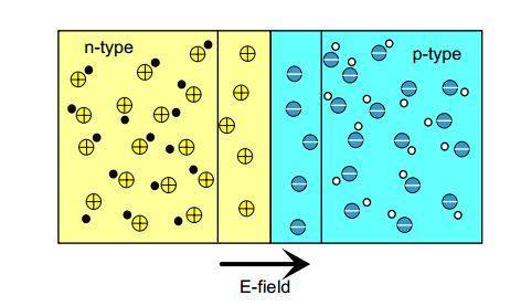
attachment.php?attachmentid=59368&stc=1&d=1370674622.jpg

Thanks for help.
 

Attachments

  • PN junction in equilibrium.JPG
    PN junction in equilibrium.JPG
    17.4 KB · Views: 545
Physics news on Phys.org
  • #2
Do you know what we call n type and p type semiconductor?

ehild
 
  • #3
ehild said:
Do you know what we call n type and p type semiconductor?

ehild

Yes, I do.
I have just watched it carefully now I see. For example in N type right next to each positive ion is an electron.
I know that the electron and positive ion are separated but I usually consider that they is an unit beacuse its net charge still zero.
 
  • #4
The p and n type regions are neutral, but the electrons and holes are free to move in the whole crystal, like the conduction electrons in a metal. The pure (intrinsic) semiconductor has only few free charge carriers, as the forbidden band, the gap between valence and conduction band is broader than the thermal energy. But adding impurity atoms which have one electron more than the host atoms (for example phosphorus in silicon) these extra electrons are very loosely connected to their atoms and the thermal energy (kT) is enough to remove them from the atom. We say that the impurities make a donor level just under the conduction band. Similarly, atoms less than one electron than silicon capture an electron from an other atom, so the "hole", the place of the missing electron moves as free positive charge carrier in the crystal. The number of doping atoms can be about 1015-1020 atoms/cm3, so they are not so many with respect to the silicon atoms.

In the depletion region, the free carriers move to the other side of the junction by diffusion, electrons to the p part and holes to the n part, leaving the ions alone. The depletion region is free from free carriers, but the concentration of the ions is the same as in the bulk of the semiconductor.

ehild
 
  • Like
Likes 1 person
  • #5


I can explain why there are so many positive and negative ions in N and P type semiconductors. In the PN junction under equilibrium, there is a difference in the number of electrons and holes between the N and P type regions. This difference is due to the different doping levels of these two regions.

In the N type region, there is an excess of electrons due to the presence of donor impurities such as phosphorus. These donor impurities have more valence electrons than the atoms in the semiconductor, so they provide extra electrons to the material. These extra electrons are responsible for the negative charge in the N type region.

On the other hand, in the P type region, there is a deficiency of electrons due to the presence of acceptor impurities such as boron. These acceptor impurities have fewer valence electrons than the atoms in the semiconductor, so they create holes in the material. These holes are responsible for the positive charge in the P type region.

In the depletion region, where the N and P type regions meet, there is a diffusion of electrons from the N type region to the P type region and a diffusion of holes from the P type region to the N type region. This diffusion process creates a region with no free carriers, known as the depletion region. However, outside of this depletion region, the excess of electrons in the N type region and the deficiency of electrons in the P type region still exist, resulting in the presence of positive and negative ions respectively.

In summary, the presence of positive and negative ions in N and P type semiconductors is a result of the different doping levels and the diffusion of carriers in the PN junction under equilibrium. These ions play a crucial role in the functioning of electronic devices based on PN junctions.
 

1. Why are there so many positive and negative ions in N and P types?

The presence of positive and negative ions in N and P types is due to the doping process used to create these types of semiconductors. Doping involves adding impurities to the semiconductor material, which creates an excess of either positive (P type) or negative (N type) charge carriers, resulting in the abundance of ions.

2. How does the number of positive and negative ions affect the behavior of N and P type semiconductors?

The number of positive and negative ions significantly impacts the conductivity and electrical properties of N and P type semiconductors. The presence of these ions creates a difference in charge concentration, which allows for the flow of current and the functioning of electronic devices.

3. What is the role of positive and negative ions in the functioning of transistors?

Transistors, which are the basic building blocks of electronic devices, rely on the presence of positive and negative ions in N and P type semiconductors. These ions act as charge carriers and allow for the amplification and control of electrical signals in the transistor.

4. Are there any other factors that contribute to the abundance of positive and negative ions in N and P type semiconductors?

In addition to the doping process, other factors such as temperature, impurity concentration, and the type of material used can affect the number of positive and negative ions in N and P type semiconductors. These factors must be carefully controlled to ensure optimal performance of the semiconductor.

5. Can the number of positive and negative ions be altered in N and P type semiconductors?

Yes, the number of positive and negative ions can be altered by adjusting the doping process or changing the impurity concentration. This allows for the customization of semiconductors for specific applications and contributes to the versatility and usefulness of these materials in electronic devices.

Similar threads

  • Introductory Physics Homework Help
Replies
13
Views
2K
  • Introductory Physics Homework Help
Replies
1
Views
715
  • Introductory Physics Homework Help
Replies
18
Views
2K
  • Introductory Physics Homework Help
Replies
6
Views
1K
Replies
30
Views
5K
Replies
3
Views
738
  • Introductory Physics Homework Help
Replies
2
Views
1K
  • Introductory Physics Homework Help
Replies
4
Views
3K
  • Introductory Physics Homework Help
Replies
5
Views
2K
  • Introductory Physics Homework Help
Replies
2
Views
1K
Back
Top