NOT Gate: Inverting Inputs & Current Flow - Help Clear Confusion!

In summary: MOSFET, it requires little charge to turn on (so no current goes into it). When the MOSFET is off, the current through the resistor R1 has no where to go, and so it has no voltage drop across it, so the V2 voltage will be present at VOUT. When the switch is turned on, current can flow through R1 to ground, and so the voltage is dropped across R1, and VOUT is switched to ground.
  • #1
nGX
5
0
From what I learned at school today..
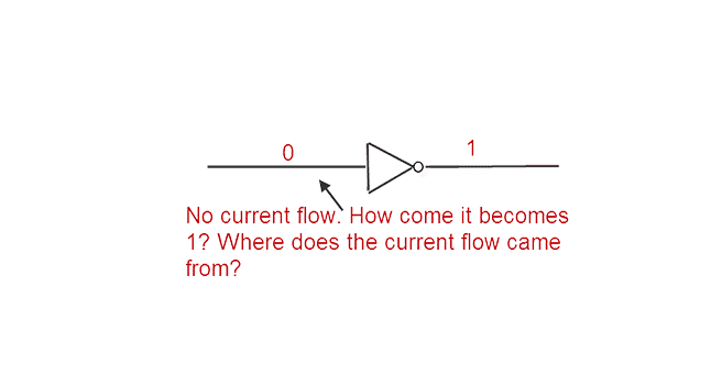
Afaik NOT gate acts as an inverter, right?
Which means if input is 0, output will be 1 and vice versa.
My question is, if input is 0 then output will be 1. From where does the gate gets its current flow? Since input is 0.
Or, it cannot be used like that? That is must be connected with AND or OR gate.

Please help me clear this confusion.

Btw, just registered. Hope to learn a lot from here.
HkMHc.png
 
Last edited:
Engineering news on Phys.org
  • #2
nGX said:
Afaik NOT gate acts as an inverter, right?
Which means if input is 0, output will be 1 and vice versa.
My question is, if input is 0 then output will be 1. From where does the gate gets its current flow? Since input is 0.
Or, it cannot be used like that? That is must be connected with AND or OR gate.

Please help me clear this confusion.

Btw, just registered. Hope to learn a lot from here.

The absence of current can be assigned the 0 meaning. 1 and 0 are mathematical abstracts, and the physical distinction between the 2 can manifest in many ways such as voltage, frequency, phase, current, position, etc.

The specific answer to your question depends on the technology and components used. Usually logic gates, including inverters, have an independent power source, and the current comes from that power source. The high and low can be given the distinction as "signals" that draw their current or voltage from a power source.
 
  • #3
Welcome to PhF!

Every kind of gate has power input in addition to the signal input. Even AND gates, which one might think could just forward their input signals. This is done because the energy loss in modern devices at their operating frequencies is enormous.
 
  • #4
DragonPetter said:
The absence of current can be assigned the 0 meaning. 1 and 0 are mathematical abstracts, and the physical distinction between the 2 can manifest in many ways such as voltage, frequency, phase, current, position, etc.

The specific answer to your question depends on the technology and components used. Usually logic gates, including inverters, have an independent power source, and the current comes from that power source. The high and low can be given the distinction as "signals" that draw their current or voltage from a power source.

Thanks for the reply. I still don't get it. Ok, let's say I'm using logic gates. What is the independent power source? A capacitor? Uh, I'm really slow. Maybe you can explain in diagrams. I'm sorry for asking too much but I really want to know.
 
  • #5
Every gate has a power line leading to the system's power supply.
 
  • #6
nGX said:
Thanks for the reply. I still don't get it. Ok, let's say I'm using logic gates. What is the independent power source? A capacitor? Uh, I'm really slow. Maybe you can explain in diagrams. I'm sorry for asking too much but I really want to know.
The independent power source could be a battery or voltage from a regulator. The power supply in a PC provides a constant set of DC voltages that power all the logic in your computer.

I attached one of the most simple ways to make an inverter. The inside of an inverter gate might look like this, but this is more simplified.

V2 is the independent voltage source. It is a constant 15V and can provide as much current as the circuit tries to pull from it.

The input is a digital pulse high-low-high-low-etc. and because the switch is a MOSFET, it requires little charge to turn on (so no current goes into it). When the MOSFET is off, the current through the resistor R1 has no where to go, and so it has no voltage drop across it, so the V2 voltage will be present at VOUT. When the switch is turned on, current can flow through R1 to ground, and so the voltage is dropped across R1, and VOUT is switched to ground.
 

Attachments

  • inverter.png
    inverter.png
    11 KB · Views: 547
  • #7
A power supply, connected to the NOT gate. A real NOT gate has 4 connections:

2 you care about in circuit designs:
- data input
- data output

And 2 you need for operation:
- "plus" and "minus", connected to a power supply

Here is an example. A and Q are the input/output, and Vdd and Vss are powering the thing.
 
  • #8
DragonPetter said:
The independent power source could be a battery or voltage from a regulator. The power supply in a PC provides a constant set of DC voltages that power all the logic in your computer.

I attached one of the most simple ways to make an inverter. The inside of an inverter gate might look like this, but this is more simplified.

V2 is the independent voltage source. It is a constant 15V and can provide as much current as the circuit tries to pull from it.

The input is a digital pulse high-low-high-low-etc. and because the switch is a MOSFET, it requires little charge to turn on (so no current goes into it). When the MOSFET is off, the current through the resistor R1 has no where to go, and so it has no voltage drop across it, so the V2 voltage will be present at VOUT. When the switch is turned on, current can flow through R1 to ground, and so the voltage is dropped across R1, and VOUT is switched to ground.
I think I got it or maybe not. The diagrams we learn in school are too simple. We don't have any power source connected to the gates(except for the input) maybe that's what made me thought of this at the first place. But looking at the diagram have made that realize that it is more than just what we learn in school, far more complex but.. somewhat interesting. It's kinda late now and I'm tired. I'll try to understand again tomorrow. But so far, I think I got an idea on how it works. (I guess)

Edit:

Here's a diagram:
 

Attachments

  • Simple NOT gate.png
    Simple NOT gate.png
    4.8 KB · Views: 573
Last edited:
  • #9
nGX said:
I think I got it or maybe not. The diagrams we learn in school are too simple. We don't have any power source connected to the gates(except for the input) maybe that's what made me thought of this at the first place. But looking at the diagram have made that realize that it is more than just what we learn in school, far more complex but.. somewhat interesting. It's kinda late now and I'm tired. I'll try to understand again tomorrow. But so far, I think I got an idea on how it works. (I guess)

Edit:

Here's a diagram:

That is a more abstracted drawing that you attached. It is not the detailed hardware implementation, but rather a logic schematic. Similar to drawing a voltage source without showing how that voltage source really works.
 
  • #10
DragonPetter said:
That is a more abstracted drawing that you attached. It is not the detailed hardware implementation, but rather a logic schematic. Similar to drawing a voltage source without showing how that voltage source really works.
Heh. I guess I have not reach that level yet. But anyway, thanks so much for your replies and patience with my questions and requests. Thanks. Things work more complicated than I ever thought of.
 
  • #11
nGX , when you take your first computer engineering class you will learn that many schematics theoretically work but cannot be implemented in real life situations. You are correct, this type of inverter is not normally used in circuits but rather an input of 1 and output of 0 inverters are used because they are more practical. The opposite situation would require the inverter to have its own independent power supply or be connected to one connected to the whole which isn't really practical.
 
  • #12
@salzrah: Inverters with 0 as the only possible output look a bit... impractical. They are not inverters, they are just constant 0.
 
  • #13
salzrah said:
nGX , when you take your first computer engineering class you will learn that many schematics theoretically work but cannot be implemented in real life situations. You are correct, this type of inverter is not normally used in circuits but rather an input of 1 and output of 0 inverters are used because they are more practical. The opposite situation would require the inverter to have its own independent power supply or be connected to one connected to the whole which isn't really practical.

Actually I'm still in high school and I'm not taking computer engineering or electronics engineering courses in the future but looking forward to software engineering. Not really interested in Physics but this topic got me a bit interested into it. Well, this and few other topics such as light, waves, radioactivity, forces (these are one of the of the chapters we learn in high school).

And, thanks for the replies. Everyone is being so friendly and informative so far. Thanks!
 
  • #14
nGX said:
Thanks for the reply. I still don't get it. Ok, let's say I'm using logic gates. What is the independent power source?
Hi nGX. Your question can be best answered by referring you to the schematic of a common digital chip, e.g., the 4049 which contains 6 of these NOT gates. http://en.wikipedia.org/wiki/Inverter_(logic_gate)

Scroll down to see an illustration of the package having 16 pins. Two are labelled "NC" which means "not connected". Of the others, twelve account for the input/output of the 6 independent gates. This leaves two pins, one marked VDD and the other VSS. What are these for? The chip has to be supplied with DC voltage to power its internal circuit, e.g., typically might supply VDD of +5v and VSS can be connected to 0v ground.
 

What is a NOT gate?

A NOT gate, also known as an inverter, is a logic gate that implements logical negation. It takes in one input and outputs the opposite value. If the input is 0, the output will be 1, and vice versa.

How does a NOT gate work?

A NOT gate works by using a transistor to invert the input signal. When the input signal is high (1), the transistor is turned off and the output is low (0). When the input is low (0), the transistor is turned on and the output is high (1).

What is the symbol for a NOT gate?

The symbol for a NOT gate is a triangle with a small circle at the end of the triangle opposite the input. The input is placed at the triangle and the output at the circle.

What is the difference between inverting inputs and current flow in a NOT gate?

Inverting inputs and current flow are two separate concepts in a NOT gate. Inverting inputs means that the output is the opposite of the input, as described earlier. Current flow refers to the direction of the current through the transistor in the NOT gate. When the input is high, the current flows from the output to the ground, and when the input is low, the current flows from the input to the output.

How can a NOT gate help clear confusion?

A NOT gate can help clear confusion by simplifying logic circuits. It can be used to convert one type of logic to another, making it easier to understand and implement. Additionally, the concept of inverting inputs and current flow in a NOT gate is an important foundation for understanding more complex logic gates and circuits.

Similar threads

Replies
16
Views
4K
  • Electrical Engineering
Replies
9
Views
3K
Replies
4
Views
1K
  • Electrical Engineering
Replies
29
Views
3K
Replies
2
Views
7K
  • Electrical Engineering
Replies
1
Views
1K
  • Electrical Engineering
Replies
16
Views
4K
  • Electrical Engineering
Replies
23
Views
4K
  • Electrical Engineering
Replies
10
Views
1K
  • Electrical Engineering
Replies
20
Views
2K
Back
Top