Reducing Gap Around IC Chip Pins for 0.5mm Track

In summary, the conversation discusses how to reduce the size of the gap around individual pins of IC chips in a PCB design project. It is recommended to adjust the clearance rules and set it to a higher priority to avoid shorts during manufacturing. The minimum clearance and trace width are dependent on the board house, with 10 mil being a common size.
  • #1
hayowazzup
64
0
Hello, I am currently working on a PCB design project,
just wondering if anybody knows how to reduce the size of the gap(the black circular region) around individual pin of IC Chips (after I have done the polygon pour)
so that a 0.5mm ground track can get through.
In addition, what is the minimum size that I could reduce it down to? does that depend on the "pcb board printer"?

unfortunately I cannot upload the image for now
but here is an example involving ic chips
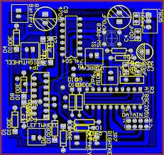

n:ANd9GcR_AEJb_ArrA6r_m6jOq4IgU5AQ5Aalsev5zxSpEPIj3e27HSU&t=1&usg=__bs0xY1-ni17-1ETuSybQbb_aep0=.jpg
 
Last edited:
Engineering news on Phys.org
  • #2
You will have to adjust your clearance rules to change this. You would enter a new rule for this specific section using the query builder and make sure to set it to a higher priority than the other clearance rules. Generally speaking, I would recommend 15-20 mils of clearance between the pads and the ground pour with TH board assemblies. This reduces the risk of shorts during manufacturing.

To answer your other question, yes, minimum clearance and trace width are functions of the board house. 10mil clearance and track width should be pretty common place, but you should always check first.
 
Last edited:

1. How do you reduce the gap around IC chip pins for 0.5mm track?

To reduce the gap around IC chip pins for 0.5mm track, you can use a technique called "micro-via stitching." This involves placing multiple small vias around the pins to create a continuous ring of copper, reducing the gap and improving the signal integrity.

2. Why is reducing the gap around IC chip pins important?

Reducing the gap around IC chip pins is important because it can improve the electrical performance of the circuit. The gap can act as an impedance discontinuity, causing reflections and signal degradation, leading to errors and malfunctions in the circuit.

3. How do you determine the optimal gap size for IC chip pins?

The optimal gap size for IC chip pins is typically determined by the manufacturer's datasheet and design guidelines. It is important to follow these guidelines to ensure proper signal integrity and functionality of the circuit.

4. Can reducing the gap around IC chip pins affect the manufacturing process?

Yes, reducing the gap around IC chip pins can affect the manufacturing process. It may require additional steps, such as micro-via stitching, which can increase the complexity and cost of production. It is important to consider these factors during the design process.

5. Are there any other techniques for reducing the gap around IC chip pins?

Yes, there are other techniques for reducing the gap around IC chip pins, such as using smaller pitch packages or using high-density interconnect (HDI) technology. However, these techniques may also come with their own challenges and considerations, so it is important to consult with a PCB designer or manufacturer for the best approach.

Similar threads

  • DIY Projects
Replies
5
Views
2K
  • DIY Projects
Replies
30
Views
4K
  • Sci-Fi Writing and World Building
2
Replies
52
Views
4K
  • General Discussion
Replies
2
Views
6K
  • Introductory Physics Homework Help
Replies
33
Views
4K
Replies
13
Views
6K
  • Aerospace Engineering
Replies
2
Views
7K
  • MATLAB, Maple, Mathematica, LaTeX
Replies
4
Views
2K
Back
Top