How Does Electron Accumulation Affect Potential Energy in MOS Capacitors?

  • Thread starter 1msm
  • Start date
  • Tags
    Charge
In summary, when a positive potential is applied to the left side metal of a MOS capacitor, it results in the accumulation of electrons on the right side of the semiconductor, causing a decrease in potential energy. This accumulation will continue until the electric fields are balanced.
  • #1
1msm
8
0
Hello everyone,

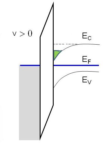
Here in below metal oxide semiconductor(MOS) capacitor,
00606.jpg

when we put positive potential on left side metal(gate), negative charge (electrons) get accumulated onto the right side semiconductor edge(as shown in green color), this results in bond bending in semiconductor and its conduction bond falls down.
So is the accumulating electrons potential energy is also falling down..??
and what happens to the next coming electrons..??
 
Physics news on Phys.org
  • #2
Thanks in advance.Yes, the potential energy of the electrons will decrease as they accumulate on the right side of the semiconductor. The next electrons will continue to accumulate until the electric field created by the applied voltage is balanced by the field created by the accumulated electrons.
 

1. What is a charge accumulation layer?

A charge accumulation layer is a region of a material where charges (electrons or holes) have accumulated due to the presence of an electric field. This can occur at the interface between two different materials or within a single material.

2. How does a charge accumulation layer form?

A charge accumulation layer forms when an electric field is applied to a material. This field causes charges to move and accumulate in a particular region, resulting in a layer of charge. The formation of this layer is dependent on the properties of the material, such as its conductivity and band structure.

3. What is the significance of a charge accumulation layer?

The presence of a charge accumulation layer can significantly affect the behavior and properties of a material. It can alter the conductivity, band structure, and other electronic properties of the material. This phenomenon is commonly utilized in electronic devices such as transistors and solar cells.

4. How is a charge accumulation layer measured or detected?

A charge accumulation layer can be measured or detected using various techniques such as Hall effect measurements, capacitance-voltage measurements, and Kelvin probe force microscopy. These methods allow researchers to directly observe and characterize the presence and behavior of the charge accumulation layer.

5. Can a charge accumulation layer be controlled?

Yes, a charge accumulation layer can be controlled through the application of an external electric field or by changing the properties of the material. This control allows for the manipulation of the material's electronic properties and can be utilized in various electronic devices and applications.

Similar threads

  • Atomic and Condensed Matter
Replies
1
Views
1K
  • Atomic and Condensed Matter
Replies
1
Views
2K
  • Atomic and Condensed Matter
Replies
1
Views
2K
  • Atomic and Condensed Matter
Replies
2
Views
2K
  • Atomic and Condensed Matter
Replies
1
Views
4K
Replies
15
Views
1K
  • Atomic and Condensed Matter
Replies
1
Views
3K
  • Electromagnetism
2
Replies
36
Views
3K
  • Atomic and Condensed Matter
Replies
8
Views
2K
  • Atomic and Condensed Matter
Replies
1
Views
1K
Back
Top