Decoupling Caps' Via Position

  • Thread starter saad87
  • Start date
  • Tags
    Position
In summary, the design involves a 4-layer board with CPLDs and a uC. The top and bottom layers are for signals, the 2nd layer is ground, and the 3rd layer is 3.3V. A 0.1uF X7R Ceramic cap in 0402 package is placed on every Vcc/Gnd pair, with the vias placed between the cap and IC pads to minimize parasitic inductance. Alternative placement methods are discussed, but the current placement is deemed ideal. A potential issue with the vias being too close together and causing shorting is addressed, with a solution of adjusting the thermal pad stack size. It is recommended to use 0.01uF caps
  • #1
saad87
85
0
I'm designing a 4-layer board with a couple of CPLDs and a uC. The top and bottom layer are for signals and the 2nd layer is ground and the 3rd layer is 3.3V.

I'm placing a 0.1uF X7R Ceramic cap in 0402 package on every Vcc/Gnd pair. The thing that confuses me is that I've seen several ways in which they are placed. I've placed them in the most obvious way, as shown below:
UDJi1.jpg


My question is: is there another arrangement that is more effective? Someone I know recommended placing the power/ground vias between the capacitor and the IC pins. Is that more effective?

Would appreciate some thoughts.
 
Engineering news on Phys.org
  • #2
Your vias are placed well. You want to minimize the parasitic inductance from the cap to the IC pads. Putting the vias between the cap and IC pads would increase the inductance. That is the beauty of the SMT decoupling caps -- being able to get them so close to minimize the parasitic inductance.
 
  • #3
I would think that placing the vias between the caps and IC pins introduces the chance that the noise you are trying to remove gets coupled onto the IC pins/decoupled traces. It also may require you move the decoupling caps out a little from the IC pins (not desirable).

I would ask them why they suggest doing that and if they don't have a good answer stick with what you have.
 
  • #4
The thing that confuses me is that I've seen several ways in which they are placed.

I believe yours is the ideal placement that also meets manufacturing rules.

You'll often see other placements in designs that deviate from the ideal because of other practical issues that pop up, usually relating to getting the circuit density higher.

For example, on a 4+ layer board a common problem is traces on the inner layers preventing the vias from going in where you would like. Or fan-in on a BGA grid to the middle balls. You could not make this structure to all of them.
 
  • #5
I take that the cap is on the other side of the board. I usually put the via a little closer to the cap to the limit of the manufacturing requirement. If they are on the same side, then looks good to me. I would use 0.01uF instead from the higher frequency components. I make it up by putting a 4.7uF cap close to the chip.
 
  • #6
Thanks for all the advice, guys! I'll stick with this layout but may have to deviate from it slightly. I'll describe the issue below. Yungman, the cap are on the same side as the chip. I was tempted to put it below, but felt the decoupling is most important. I also have 47uF caps about 2-3 inches from the chips as bulk capacitance. These caps are Tantulum.

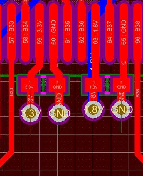
One issue that I realized is that I can't place the vias too close together. Suppose I have a 3.3V and a GND via. The 3.3V connects to the 3.3V plane using a thermal relief. However, the GND via is running very close to it and sometimes the dead-copper around this via runs into the thermal-relief. They are not shorting, my EDA package would tell me if they were. I will provide a picture in a few hours - I'm not on my computer at the moment.

I've managed to fix this in areas where I'm not decoupling and hence the via distance isn't too much of an issue. I'm a bit reluctant to do this on vias which connect the decoupling caps - but should I move the vias a couple of mills apart? Is this a big issue or makes no difference?
 
  • #7
saad87 said:
Thanks for all the advice, guys! I'll stick with this layout but may have to deviate from it slightly. I'll describe the issue below. Yungman, the cap are on the same side as the chip. I was tempted to put it below, but felt the decoupling is most important. I also have 47uF caps about 2-3 inches from the chips as bulk capacitance. These caps are Tantulum.

One issue that I realized is that I can't place the vias too close together. Suppose I have a 3.3V and a GND via. The 3.3V connects to the 3.3V plane using a thermal relief. However, the GND via is running very close to it and sometimes the dead-copper around this via runs into the thermal-relief. They are not shorting, my EDA package would tell me if they were. I will provide a picture in a few hours - I'm not on my computer at the moment.

I've managed to fix this in areas where I'm not decoupling and hence the via distance isn't too much of an issue. I'm a bit reluctant to do this on vias which connect the decoupling caps - but should I move the vias a couple of mills apart? Is this a big issue or makes no difference?

I know exactly what you mean as I fight this problem. I layout most of my boards ( say all!) as layout is the most important part of the design and you need to know the circuit to do it. Go to pad stack and define the pad size of the thermal. A lot of the default pad size of thermal are bigger than the regular vias, this to me is stupid. You can reduce the size, define the ring to less than 5mils, set the spoke width to 15mils. I just make the inner pad of the thermal same size as the normal via size.BUT in your picture, I don't see a big thermal, so I don't see your problem. I am saying in general case that I would fix the default thermal pad stack.

Regarding to 0.1uF, use 0.01uF instead because it is better in bypassing the high frequency. You should use 4.7uF first before 47uF. I don't usually put 47uF for each IC and it is not needed. One 4.7 uF for each IC is enough, just make sure you have 0.01 on every power pin.
 
  • #8
yungman said:
Regarding to 0.1uF, use 0.01uF instead because it is better in bypassing the high frequency.

I think the OP's application is not super-high-frequency, so the 0.1uF caps may work fine. I use 0.1uF SMT caps in our designs for digital decoupling, and our EMI and signal integrity measurements are pretty good. I think 0.01uF may work better for very high frequency circuits like DRAM arrays and such. Keeping the parasitic inductance low with the layout like we're talking about keeps the SRF reasonably high, even with 0.1uF caps.

It would be interesting to do an EMI comparison between 0.1uF and 0.01uF caps in a design sometime... Maybe I'll put that on my to-do list (but not very high at the moment) :smile:
 
  • #9
Here's the picture I promised, but it seems yungman already provided a solution :):

7gTIX.jpg


As berkeman said, I don't have a high frequency requirement. So I feel 0.1uF would be OK. Regarding 47uF, I'm using an Altera CPLD and they recommend 0.01 to 0.1uF decoupling and 47uF to 100uF for bulk capacitance about 2-3 inches away and finally a 1000uF cap somewhere on the board.
 
  • #10
yungman said:
Regarding to 0.1uF, use 0.01uF instead because it is better in bypassing the high frequency.
This is questionable advice. The package size (i.e. the parasitic inductance) is the driving factor that determines how effective the decoupling capacitor is at higher frequencies. I've plotted the mentioned values in 0603 sizes with TDK's Component Characteristics Viewer and I, for one, wouldn't sacrifice the obvious benefit at low frequencies for that narrow band where the 0.01uF cap is superior.

The best advice on this topic that I've seen, is this: choose the smallest package that is practical for the application and then choose the largest capacitance value that is available in that package size (or perhaps the second largest to avoid availability/lead-time problems).

691EYVb.png


Comments are welcomed (of course).

Image source: http://www.tdk.co.jp/ccv/index.asp
 

1. What are decoupling caps and why are they important?

Decoupling caps, also known as decoupling capacitors, are electronic components that are used to stabilize the power supply in a circuit. They serve as a temporary energy source to provide a steady flow of electricity to sensitive components, preventing any fluctuations or noise that may interfere with the circuit's proper functioning.

2. How do decoupling caps work?

Decoupling caps work by storing electrical charge and releasing it when needed. They act as a buffer between the power source and the circuit, reducing the effects of electrical noise and ripple voltage. They also help to maintain a constant voltage level, ensuring that the circuit operates within its specified limits.

3. Where should decoupling caps be placed on a circuit board?

Decoupling caps should be placed as close as possible to the power and ground pins of the sensitive components they are protecting. This means that they should be placed near the ICs (integrated circuits) or other components that require a stable power supply. Ideally, each sensitive component should have its own decoupling cap.

4. What are the consequences of improper placement of decoupling caps?

If decoupling caps are not placed correctly, they may not be able to provide the necessary energy to stabilize the power supply, leading to noise and voltage fluctuations in the circuit. This can cause malfunctions, data errors, and even damage to the components. In extreme cases, it can also lead to electromagnetic interference (EMI) and affect the performance of other nearby circuits.

5. How do I choose the right decoupling caps and via positions for my circuit?

The choice of decoupling caps and via positions depends on various factors such as the circuit's power requirements, the frequency of operation, and the type of components used. It is essential to consult the datasheet of the components and follow the recommended guidelines for decoupling and via placement. Additionally, simulation tools can be used to optimize the placement for maximum performance.

Similar threads

  • Electrical Engineering
Replies
23
Views
4K
Replies
16
Views
29K
  • Electrical Engineering
Replies
2
Views
5K
Back
Top