Electronic NOT gate chip question

In summary: What do you mean it can only sink current? So is anything flowing from the 15V or not? And what does this mean for Q when it is high?Thanks for the clarification!The 74HC74 is a CMOS version, the the output is build using only cmos invertter. And at first glance you can treat it as ideal switch with some resistance.And the switch can connect Q to Vcc or to GND.And now if we get CMOS inverter (NOT) gate and connect input node to positive terminal of a power supply.So we have input at "high," or in a binary "1" state and the output is in "low" state or
  • #1
tim9000
867
17
Hi,

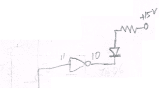
Can current flow both ways through a NOT gate, or is the diagram I saw, much like the picture I drew here, just drawn the wrong way around?
not.png

Anyway, say it was correct, so what does this mean? Because the chip itself (the not gate chip Vcc = 5V and Gnd) takes 5V between it and the chip ground. So when the 15V is active, pin 11 gets inverted to 0V? and When 15V is not active, what is pin 11? Is it then 5V? (So it is never 15V?)

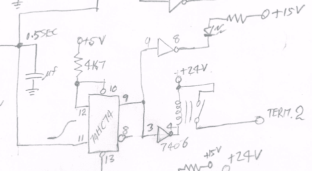
For a larger context on what I'm trying to figure out:
1111111.PNG

It seems like the not gates and the LED and relay coil, are flowing backwards? Because Pin 9 of the flip flop is Q.
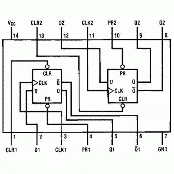
How does the current flow to or from pin 9? If pin 9 is high because it was pulsed with data on the clock then presumably pin 9 is 5V? (from Pin 12 and pin 10)? But 5V with reference to what ground?

Where the chip is:
92111-74HC74-D-type-Flip-Flop-Pic002-700x700.GIF

Thanks!
(I can provide more info on the diagram if needed)
 
Engineering news on Phys.org
  • #2
It is a design error to pull the output of a logic gate above its power supply. That can lead to latch-up of the gate, destroying it (with smoke usually)...
 
  • #3
This is not a design error. The 7406 is a open-collector gate. And that means that 7406 can only sink current.
 
  • #4
Jony130 said:
This is not a design error. The 7406 is a open-collector gate. And that means that 7406 can only sink current.
Oops, I didn't check that. Thanks for the correction! :smile:

Can it handle 24V, though? And that coil drive without a flyback protection diode looks to be a problem...
 
  • #6
berkeman said:
Looks like the 7406 can handle 30V at its output. Still, the coil drive without the catch diode looks to be a problem.

http://www.ti.com.cn/cn/lit/ds/symlink/sn7406.pdf

I think the bottom relay had a flyback protection diode, that would look like this wouldn't it:
upload_2016-6-9_1-52-15.png

I don't know why the other two didn't...

What do you mean it can only sink current? So is anything flowing from the 15V or not? And what does this mean for Q when it is high?

Cheers
 
  • #7
The 74HC74 is a CMOS version, the the output is build using only cmos invertter. And at first glance you can treat it as ideal switch with some resistance.
And the switch can connect Q to Vcc or to GND.
6.jpg


And now if we get CMOS inverter (NOT) gate and connect input node to positive terminal of a power supply.
So we have input at "high," or in a binary "1" state and the output is in "low" state or binary "0".
15.png

So output of a gate is now "sink" the current to provide a "0" or "low" state at the output. Vout is almost equal GND.

And now see what happens if we reverse the input's logic level to a binary "0", "low".
The output now must be in "High" binary "1" state. So output of a gate is "sourcing" the output current. And output voltage is almost equal VDD.
15b.png
 
  • Like
Likes berkeman
  • #8
tim9000 said:
What do you mean it can only sink current? So is anything flowing from the 15V or not? And what does this mean for Q when it is high?
Do you know what the output stage of an open-collector gate looks like? Check out the 7406 datasheet "schematic" for more info.
 
  • #9
Thanks for the great replies!
Jony130 said:
The 74HC74 is a CMOS version, the the output is build using only cmos invertter. And at first glance you can treat it as ideal switch with some resistance.
And the switch can connect Q to Vcc or to GND.
View attachment 101813

And now if we get CMOS inverter (NOT) gate and connect input node to positive terminal of a power supply.
So we have input at "high," or in a binary "1" state and the output is in "low" state or binary "0".
View attachment 101814
So output of a gate is now "sink" the current to provide a "0" or "low" state at the output. Vout is almost equal GND.

And now see what happens if we reverse the input's logic level to a binary "0", "low".
The output now must be in "High" binary "1" state. So output of a gate is "sourcing" the output current. And output voltage is almost equal VDD.
View attachment 101815
Okay, so that means that Q is either 5V as supplied by Vcc (not pin 12) or zero, as supplied by Gnd.
I'm still struggling to come to terms with the NOT gate. So this means that the back end of the not gate is acting like a switch to, for instance, make pin 9, when Q is 5V, (become inverted to zero volts) sinking the 15V to Gnd and make the LED turn on? And make Pin 4 (of that NOT gate) sink the 24V and turn on the relay?

berkeman said:
Do you know what the output stage of an open-collector gate looks like? Check out the 7406 datasheet "schematic" for more info.
I'll look that up in the morning, it's almost 3am here.

Thanks!

P.S. So what did the flyback diode (as highlighted in #6) do? (Why is it necessary?)
 
  • #10
tim9000 said:
So what did the flyback diode (as highlighted in #6) do? (Why is it necessary?)
Without it, when the pulldown transistor in the drive gate opens up (to turn off the coil current), you get a large positive voltage spike at the bottom of the inductor, which can blow up the output transistor.

https://en.wikipedia.org/wiki/Flyback_diode
 
  • #11
tim9000 said:
Okay, so that means that Q is either 5V as supplied by Vcc (not pin 12) or zero, as supplied by Gnd.
Yes, Q can be at 5V (almost, load dependent) supplied by Vcc/Vdd (pin 14). And Q can be 0V also (supplied by Gnd pin 8)

tim9000 said:
I'm still struggling to come to terms with the NOT gate. So this means that the back end of the not gate is acting like a switch to, for instance, make pin 9, when Q is 5V, (become inverted to zero volts) sinking the 15V to Gnd and make the LED turn on? And make Pin 4 (of that NOT gate) sink the 24V and turn on the relay
Normally the inputs are "voltage driven", almost no input current is needed for CMOS (I_IL = 1.6mA ; I_IH = 0.04mA max for TTL gates ).
So, when the pin 9 is at +5V (high state) the inverter (NOT gate) will open his BJT at the output (the output is short via saturated transistor to pin 8/GND). The "output switch" can only short to GND in "open-collector gates". Therefore the current from +15V will start to flow :
+15V----->Resistor---LED----> pin 10 (NPN transistor)----> pin 8 ----> -15V (GND). And we have the same situation the the relay. But this time the current is supplied by 24V source.
 
  • #12
I don't think I've ever had such a succinctly helpful post before.
berkeman said:
Without it, when the pulldown transistor in the drive gate opens up (to turn off the coil current), you get a large positive voltage spike at the bottom of the inductor, which can blow up the output transistor.

https://en.wikipedia.org/wiki/Flyback_diode
Yes, that is something to consider, I suppose I just didn't expect that even such tiny silicon switches and small relay coils deserve the same treatment as large inductors.

Jony130 said:
Normally the inputs are "voltage driven", almost no input current is needed for CMOS (I_IL = 1.6mA ; I_IH = 0.04mA max for TTL gates ).
So, when the pin 9 is at +5V (high state) the inverter (NOT gate) will open his BJT at the output (the output is short via saturated transistor to pin 8/GND). The "output switch" can only short to GND in "open-collector gates". Therefore the current from +15V will start to flow :
+15V----->Resistor---LED----> pin 10 (NPN transistor)----> pin 8 ----> -15V (GND). And we have the same situation the the relay. But this time the current is supplied by 24V source.
Interesting about the CMOS.
Brilliant reply, and I'm so close to fully grappling with it. But I have a couple questions, (I looked up Open Collector on wiki) so are you saying that in the state pictures for #7, there is a PNP BJT at the output that isn't seen?
what do you mean -15V? Isn't it just +15V and zero V for GND?
I was thinking so pin 9 is ~ 5V, it'd be:
+15V----->Resistor---LED---->Pin 10 ----> Pin 7 GND (so GND is pin 7 of the 'NOT chip', not seen in our diagram)
What was the pin 8 you were talking about?

Thanks heaps
 
  • #13
tim9000 said:
Brilliant reply, and I'm so close to fully grappling with it. But I have a couple questions, (I looked up Open Collector on wiki) so are you saying that in the state pictures for #7, there is a PNP BJT at the output that isn't seen?

no, as can be seen, there is a P channel and a N channel MOSFET on the output ( because these are CMOS examples )If they were standard TTL then it would have BJT transistor outputs
look at the diagrams on this page .,.. easier than me explaining it :)

http://www.radio-electronics.com/in...-ic-families-technologies/7400-series-ttl.phpDave
 
  • #14
davenn said:
no, as can be seen, there is a P channel and a N channel MOSFET on the output ( because these are CMOS examples )If they were standard TTL then it would have BJT transistor outputs
look at the diagrams on this page .,.. easier than me explaining it :)

http://www.radio-electronics.com/in...-ic-families-technologies/7400-series-ttl.phpDave
I didn't think so, what did Jony123 mean by BJT and PNP then?
Cheers

P.S. Thanks for the link
 
  • #15
tim9000 said:
I didn't think so, what did Jony123 mean by BJT and PNP then?

presumably you were referring to this ...

Jony130 said:
Normally the inputs are "voltage driven", almost no input current is needed for CMOS (I_IL = 1.6mA ; I_IH = 0.04mA max for TTL gates ).
So, when the pin 9 is at +5V (high state) the inverter (NOT gate) will open his BJT at the output (the output is short via saturated transistor to pin 8/GND). The "output switch" can only short to GND in "open-collector gates". Therefore the current from +15V will start to flow :
+15V----->Resistor---LED----> pin 10 (NPN transistor)----> pin 8 ----> -15V (GND). And we have the same situation the the relay. But this time the current is supplied by 24V source.

the bit bolded is a little confusing as he is referring to CMOS and TTL in the same sentence but the rest of the comments
should be referring to a TTL output

hopefully he will return and clarify his comments :smile:Dave
 
  • #16
davenn said:
presumably you were referring to this ...
the bit bolded is a little confusing as he is referring to CMOS and TTL in the same sentence but the rest of the comments
should be referring to a TTL output

hopefully he will return and clarify his comments :smile:Dave
Sort of, I was also thinking of:
Jony130 said:
will open his BJT at the output (the output is short via saturated transistor to pin 8/GND). The "output switch" can only short to GND in "open-collector gates". Therefore the current from +15V will start to flow :
+15V----->Resistor---LED----> pin 10 (NPN transistor)

Indeed.
Cheers!
 
  • #17
tim9000 said:
so are you saying that in the state pictures for #7, there is a PNP BJT at the output that isn't seen?
Sorry for confusing you. Post #7 shows CMOS gate 74HC/74HCT family or CD4000 family. And in CMOS we have a P-Channel MOSFET (the upper one ) and N-Channel MOSFET (lower transistor). The NOT gate (7406) is TTL circuit - Transistor-Transistor-Logic (BJT only).

tim9000 said:
what do you mean -15V?
Negative terminal of a 15 supply

tim9000 said:
+15V----->Resistor---LED---->Pin 10 ----> Pin 7 GND (so GND is pin 7 of the 'NOT chip', not seen in our diagram)
Very good. And we draw a circuit that contains an logic circuit or a opamp we very often skip the power supply on the diagram to make the circuit more easy to analysis. But we have to kept in mind that every circuit needs a power supply.

tim9000 said:
What was the pin 8 you were talking about?
My mistake, I meant pin 7.
 
  • #18
Jony130 said:
Negative terminal of a 15 supply

just be careful with your terminology in future :wink:
as -15V is a negative 15V rail of a split rail PSU, which is very different to a 0V rail of a single rail PSUDave
 
  • #19
Jony130 said:
My mistake, I meant pin 7.
Yeah I think I understand, because they're all (all the ICs) fed by the same positive rail and grounded by the same earth, we can omit them somewhat in the digram.

Jony130 said:
Negative terminal of a 15 supply
davenn said:
just be careful with your terminology in future :wink:
as -15V is a negative 15V rail of a split rail PSU, which is very different to a 0V rail of a single rail PSU
Wait, so is -15v the same as 0v? Or not?
It's Ground right?
Because I would think that +15V to -15V is a 30V potential...
I didn't remember a -15V rail in the diagram.

Thanks
 
  • #20
tim9000 said:
Yeah I think I understand, because they're all (all the ICs) fed by the same positive rail and grounded by the same earth, we can omit them somewhat in the digram.
Wait, so is -15v the same as 0v? Or not?
It's Ground right?
Because I would think that +15V to -15V is a 30V potential...
I didn't remember a -15V rail in the diagram.

Thanks

again jony130 was a bit unclear
In this case he really meant the 0V / negative terminal of the PSU, NOT -15V
This is why I was telling him to be careful with his terminology so as to avoid the sort of confusion that resulted in the above posts

It's Ground right?

no, it's just 0V ... ground (GND) refers to a different situation where the 0V rail is connected say to the metal chassis which may or may not be connected to a physical ground via the mains or other cabling. There was a thread on here some time ago discussing the various types of grounds, the misuse of the term etc
Dave
 
  • #21
davenn said:
no, it's just 0V ... ground (GND) refers to a different situation where the 0V rail is connected say to the metal chassis which may or may not be connected to a physical ground via the mains or other cabling. There was a thread on here some time ago discussing the various types of grounds, the misuse of the term etc
In "modern" electronics we can have a ground without any metal chassis. Simply, the ground is a reference point in respect of which we are measure all voltage in the circuit. And if a Negative terminal (PSU) is used as a our reference point, we can declare this point as a ground. But I'm sure you already know this.
To measure the voltage we need two point in the space. One of this point is treat as a reference point. We have a very similarity situation when we try to measure a height of an object. We need a reference point. The most common reference pint is "above mean sea level". But when you measure the height of the table in your house the floor now becomes your reference point.
0.1.PNG
 
  • #22
Jony130 said:
In "modern" electronics we can have a ground without any metal chassis. Simply, the ground is a reference point in respect of which we are measure all voltage in the circuit. And if a Negative terminal (PSU) is used as a our reference point, we can declare this point as a ground. But I'm sure you already know this.

and that is exactly what I was commenting on as a misuse of the term :smile:
It;s just the point you are going to make as your reference but to which all other points of potential ( positive or negative to that reference) are referred back toD
 
  • #23
Yeah, in an offline switch-mode power supply product I'm working on right now, we have at least three "grounds" that we keep track of. Two on the primary side labeled PGND and NGND, and one on the secondary side labeled ISOGND. At the moment, we are not connecting the external Earth ground to any of these internal ground nets. Each ground symbol in our schematic is labeled so that we can keep track of things... :smile:
 
  • Like
Likes davenn
  • #24
berkeman said:
Two on the primary side labeled PGND and NGND, and one on the secondary side labeled ISOGND.
and you don't have a digital ground as well ?? haha :wink:
 
  • #25
davenn said:
and you don't have a digital ground as well ?? haha :wink:
No but we do have a couple of bead-isolated analog supplies on both sides of the isolation barrier. Always watching out for shared impedance noise. :smile: Thanks brother.
 
  • #26
davenn said:
no, it's just 0V ... ground (GND) refers to a different situation where the 0V rail is connected say to the metal chassis which may or may not be connected to a physical ground via the mains or other cabling. There was a thread on here some time ago discussing the various types of grounds, the misuse of the term etc
Dave
That seems a bit strange, because as far as I was aware, Earth was connected to the metal chassis. Ok national standard aside, what if I said instead that the GND 0V rail is the same as neutral?

Thanks
 
  • #27
tim9000 said:
That seems a bit strange, because as far as I was aware, Earth was connected to the metal chassis.

That may, but not necessarily, be true for a piece of mains powered equip where the mains Earth is connected to the equip metal chassis
it should always be for direct mains powered gear ... I don't know the specific electrical codes
it may or may not be if the mains voltage goes through a step-down transformer. I personally always wire in the mains Earth to the chassis
but I have seen commercial gear that hasn't been
tim9000 said:
if I said instead that the GND 0V rail is the same as neutral?

no, The term Neutral is specifically used for mains AC wiring
in household wiring ( at least) the neutral is normally connected to Earth ground at the power fuse board/meter box

the term neutral is NOT used for low voltage AC say on the secondary side of a transformer
it is also NOT used for the negative / 0 V rail of a DC supply
Dave
 
  • #28
Okay, I didn't realize this thread had spilt over onto a second page, I missed all the posts up to my last reply, on this page.
So the point is that GND is really a theoretical concept we're working on within a scope, of 0V? (relative to everything else in it's scope)

Thanks
 
  • #29
it's just a way of stating a 0V position
Jony130 showed with those stacks of batteries that it is just a place where you decide to make the 0V reference
Berkeman showed there are a number of GND references and I teased him on yet another one

so a circuit can have a number of specific grounds depending on the situation
analog ground AGND, digital ground DGND, PGND, NGND and ISOGND

I am not too familiar with those last 3Dave
 

1. What is an Electronic NOT gate chip?

An electronic NOT gate chip is a digital logic chip that performs the logical operation of negation. It takes in a single input and produces an inverted output, meaning that if the input is high (1), the output will be low (0) and vice versa. It is commonly used in digital circuits to control the flow of information.

2. How does an Electronic NOT gate chip work?

An electronic NOT gate chip works by using transistors to manipulate the input voltage. When the input is high, the transistors will be in a non-conducting state, resulting in a low output. When the input is low, the transistors will be in a conducting state, resulting in a high output. This inversion of the input voltage is what gives the NOT gate its name.

3. What is the symbol for an Electronic NOT gate chip?

The symbol for an electronic NOT gate chip is a triangle with a small circle at the point and the input and output lines attached to the other two sides of the triangle. This symbol is commonly used in digital circuit diagrams to represent the NOT gate.

4. Can an Electronic NOT gate chip be used in combination with other logic gates?

Yes, an electronic NOT gate chip can be used in combination with other logic gates to create more complex logic functions. It is often used in combination with other gates such as AND, OR, and XOR gates to perform various logical operations.

5. What are some common applications of Electronic NOT gate chips?

Electronic NOT gate chips are commonly used in digital electronics, such as in microprocessors, computers, and electronic circuits. They are also used in communication systems, control systems, and in various industrial and consumer electronics products. They play a crucial role in performing logic operations and controlling the flow of information in these devices.

Similar threads

  • Electrical Engineering
Replies
19
Views
3K
  • Electrical Engineering
Replies
34
Views
4K
  • Electrical Engineering
Replies
16
Views
4K
  • Electrical Engineering
Replies
6
Views
1K
  • Engineering and Comp Sci Homework Help
Replies
20
Views
2K
  • Electrical Engineering
Replies
13
Views
6K
  • Sticky
  • Programming and Computer Science
Replies
13
Views
4K
  • Electrical Engineering
Replies
31
Views
7K
Replies
5
Views
3K
  • Electrical Engineering
Replies
24
Views
8K
Back
Top