- #1
Sciencestd
- 63
- 9
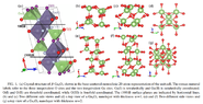
I have three questions regarding the material Gallium Oxide. I was reading in several articles and they introduced its structure as it has monoclinic structure and it consists tetrahedral and octahedral structures in it. What I can't understand I can connect this structure to the chemical formula: Ga2O3... because in octahedral or tetrahedral the gallium is bonded to 4 or 6 oxygen atoms.
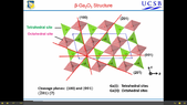
My second question is: how the plane 100 or 001 in the pictures below is crossing the unit cell I can't read this actually?
My last question is regarding the material, that it is a n-type semiconductor... Why it should be n-type if all the oxygen atoms are bonded with gallium atoms? why should be free electrons in the conduction band even there is no doping?!The first image is from the article: https://journals.aps.org/prb/pdf/10.1103/PhysRevB.96.081409
The second image is from the presentation: https://www.spiedigitallibrary.org/...ce-Presentation/10.1117/12.2292778.full?SSO=1