How does the dry process work using porous silicon?

In summary, The conversation discusses the use of porous silicon in the wet and dry methods for thermal oxidation. The wet method involves using electrochemical processes to allow water molecules to diffuse into the porous silicon, while the dry method remains unclear in the literature and requires further understanding of how it works. Both methods aim to prevent collapse of the cavity structure. See attachments 01 and 02 for visual examples.
  • #1
LUFER
4
0
I'm having trouble finding in the literature specifically about the porous silicon process using the dry method instead of the more common wet method that is used.
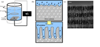
wet process
Using porous silicon to promote wet thermal oxidation uses the process electrochemically will allow water molecules to diffuse into it. Wet oxide is often used for oxide growth. So that the structure (cavities) does not collapse after using the previously mentioned process or remove that PENTAN.
Example: See the photo in attachment 01

dry process
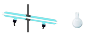
If it refers to the dry process, I can't find anything profound in the literature, it just cites the case. I would need to understand how this process works, the little I understood is that it uses two flasks where there is a cylindrical flask where there is an inlet and an outlet and the other flask where the Porous Silicon is used. If anyone can help me where I can find the literature.

Example: See the photo in attachment 02
 

Attachments

  • 01.png
    01.png
    18.6 KB · Views: 86
  • 02.png
    02.png
    3.2 KB · Views: 78

1. How does the dry process create porous silicon?

The dry process for creating porous silicon involves using a plasma etching technique. This involves exposing a silicon wafer to a gas plasma, which causes the silicon to be etched away and create pores. The gas used in the plasma etching process can vary, but commonly used gases include SF6, CF4, and CHF3.

2. What is the purpose of creating porous silicon?

Porous silicon has a high surface area and unique optical and electrical properties, making it useful for various applications in electronics, photonics, and biotechnology. It can also be used as a template for creating other materials, such as nanowires.

3. How does the dry process differ from the wet process in creating porous silicon?

The main difference between the dry and wet processes for creating porous silicon is the use of a plasma etching gas in the dry process, while the wet process involves using a chemical etchant, typically a mixture of hydrofluoric acid and an oxidizing agent. The dry process is faster and more controllable, but it requires specialized equipment.

4. What are the advantages of using porous silicon in electronic devices?

Porous silicon has a higher surface area compared to regular silicon, which allows for more efficient charge transfer and can improve the performance of electronic devices. It also has a tunable refractive index, making it useful for creating optical components. Additionally, porous silicon is biocompatible, making it suitable for use in biomedical devices.

5. Are there any limitations or challenges with using the dry process to create porous silicon?

One limitation of the dry process is that it can only be used on single-crystal silicon wafers, which are more expensive than other types of silicon. Additionally, the plasma etching process can cause damage to the surface of the silicon, which can affect the properties of the resulting porous silicon. Controlling the pore size and distribution can also be challenging in the dry process.

Similar threads

Replies
3
Views
17K
  • Mechanics
Replies
4
Views
5K
Replies
4
Views
2K
  • General Discussion
2
Replies
65
Views
11K
  • MATLAB, Maple, Mathematica, LaTeX
Replies
3
Views
265
  • Introductory Physics Homework Help
Replies
7
Views
5K
  • Art, Music, History, and Linguistics
Replies
1
Views
1K
  • Sci-Fi Writing and World Building
Replies
2
Views
2K
Replies
3
Views
34K
  • Introductory Physics Homework Help
Replies
2
Views
11K
Back
Top