Psinter
- 278
- 787
Hello, I'm new to logic circuits and I was making a 4 bit binary adder and I thought I could maybe simplify it. However, I can't find anything simpler than what I already got. What I wanted to know is: is my circuit already in its most simple form or am I making something wrong in my attempts to simplificate it (meaning it can still be simplificated)?
The circuit works as follows:
We have the 1st 4 bit number: ABCD
We have the 2nd 4 bit number: EFGH
The total sum with one bit at a time would be: (D + H) and (C + G) and (B + F) and (A + E). In other words:
ABCD
EFGH
---------
XXXX
where, (D + H) is the only one that doesn't receive any carry because it's the initial point.
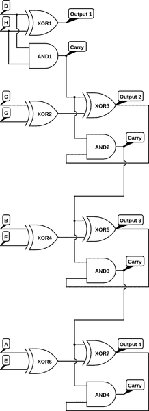
So I need 4 outputs with their respective carries as illustrated:

As you can see the pattern of circuits start at the second sum. Meaning, (C + G), (B + F), and (A + E) are the same circuits. I tried to simplify 1 of them so I could simplify the rest of the adder. However, I can't find any way to simplify it any further. When I look at the Karnaugh Map I made out of the Truth Table of the circuit that repeats I don't know what to do from there because I don't have any mapping groups there.
Truth Table: ((C \oplus G) \oplus CARRY) \wedge CARRY
\begin{array}{|c|c|c|c|}
\hline
C & G & CARRY & F1 \\ \hline
0 & 0 & 0 & 0 \\ \hline
0 & 0 & 1 & 1 \\ \hline
0 & 1 & 0 & 0 \\ \hline
0 & 1 & 1 & 0 \\ \hline
1 & 0 & 0 & 0 \\ \hline
1 & 0 & 1 & 0 \\ \hline
1 & 1 & 0 & 0 \\ \hline
1 & 1 & 1 & 1 \\
\hline
\end{array}
Karnaugh Map: ((C \oplus G) \oplus CARRY) \wedge CARRY
\begin{array}{|c|c|c|c|c|c|}
\hline
& G \wedge CARRY & 00 & 01 & 11 & 10 \\ \hline
C & & & & & \\ \hline
0 & & & 1 & & \\ \hline
1 & & & & 1 & \\
\hline
\end{array}
Does all this mean that I cannot simplify my adder any further?
The circuit works as follows:
We have the 1st 4 bit number: ABCD
We have the 2nd 4 bit number: EFGH
The total sum with one bit at a time would be: (D + H) and (C + G) and (B + F) and (A + E). In other words:
ABCD
EFGH
---------
XXXX
where, (D + H) is the only one that doesn't receive any carry because it's the initial point.
So I need 4 outputs with their respective carries as illustrated:
As you can see the pattern of circuits start at the second sum. Meaning, (C + G), (B + F), and (A + E) are the same circuits. I tried to simplify 1 of them so I could simplify the rest of the adder. However, I can't find any way to simplify it any further. When I look at the Karnaugh Map I made out of the Truth Table of the circuit that repeats I don't know what to do from there because I don't have any mapping groups there.
Truth Table: ((C \oplus G) \oplus CARRY) \wedge CARRY
\begin{array}{|c|c|c|c|}
\hline
C & G & CARRY & F1 \\ \hline
0 & 0 & 0 & 0 \\ \hline
0 & 0 & 1 & 1 \\ \hline
0 & 1 & 0 & 0 \\ \hline
0 & 1 & 1 & 0 \\ \hline
1 & 0 & 0 & 0 \\ \hline
1 & 0 & 1 & 0 \\ \hline
1 & 1 & 0 & 0 \\ \hline
1 & 1 & 1 & 1 \\
\hline
\end{array}
Karnaugh Map: ((C \oplus G) \oplus CARRY) \wedge CARRY
\begin{array}{|c|c|c|c|c|c|}
\hline
& G \wedge CARRY & 00 & 01 & 11 & 10 \\ \hline
C & & & & & \\ \hline
0 & & & 1 & & \\ \hline
1 & & & & 1 & \\
\hline
\end{array}
Does all this mean that I cannot simplify my adder any further?