Draw a NAND-gate to get that output

  • Context: MHB 
  • Thread starter Thread starter mathmari
  • Start date Start date
  • Tags Tags
    Output
Click For Summary

Discussion Overview

The discussion revolves around constructing a circuit using only NAND gates to achieve a specific logical output based on four inputs (a, b, c, d). The output is defined by the expression $[(a \lor b) \lor (c \lor \neg d)] \land (c \land \neg a)$. Participants explore how to express logical operations using NAND gates, particularly focusing on how to implement negation and conjunction.

Discussion Character

  • Technical explanation
  • Mathematical reasoning
  • Debate/contested

Main Points Raised

  • One participant suggests that the expression can be transformed using NAND gates and asks how to handle the negation in the context of the given expression.
  • Another participant confirms that inverters can be applied before and after a NAND gate, allowing for the expression of conjunctions in terms of NAND operations.
  • Participants discuss the representation of negation using NAND gates, specifically noting that $\neg a$ can be expressed as $a \text{ NAND } a$.
  • There is a proposal to simplify the expression before drawing the circuit, with some participants expressing confusion about which form of the expression to use for the drawing.
  • One participant suggests starting with an expression that has not been fully expanded to avoid duplication of variables in the circuit diagram.
  • Another participant questions whether to consider the expression in its current form or to expand it further for clarity in the circuit design.

Areas of Agreement / Disagreement

Participants generally agree on the methods for expressing logical operations using NAND gates, but there is uncertainty regarding the best approach to simplify the expression for drawing the circuit. Multiple viewpoints exist on whether to expand the expression or keep it in a simpler form.

Contextual Notes

Some participants express confusion about the implications of expanding expressions and how that affects the drawing of the circuit. There is a lack of consensus on the optimal form of the expression to use for the final circuit representation.

mathmari
Gold Member
MHB
Messages
4,984
Reaction score
7
Hey! 😊

I want to draw a circuit that has four inputs a, b, c, d, and which gives the value $[(a \lor b) \lor (c \lor \neg d)] \land (c \land \neg a)$ at the output, using exclusively the NAND gates with two inputs.
Hint: If you connect the two inputs of such a NAND gate, you get a so-called inverter, i.e. a circuit implementation of the logical negation.

The NAND-gate is:
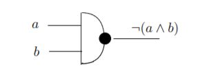
nand.JPG


I have done the following:
\begin{align*}[(a\lor b)\lor (c\lor \neg d)]\land (c\land \neg a)&=[\neg (\neg a\land \neg b)\lor \neg (\neg c\land d)]\land (c\land \neg a)\\ & =\neg [(\neg a\land \neg b)\land (\neg c\land d)]\land (c\land \neg a)\end{align*}
We can get the part $\neg [(\neg a\land \neg b)\land (\neg c\land d)]$ using the NAND gate, right? What about the second part? Do we have to write it in an other way? :unsure:
 
Physics news on Phys.org
mathmari said:
We can get the part $\neg [(\neg a\land \neg b)\land (\neg c\land d)]$ using the NAND gate, right? What about the second part? Do we have to write it in an other way?
Hey mathmari!

Yep.
We can apply inverters both before and after a NAND gate can't we?
That is, we can write $x\land y$ as $\lnot\lnot(x\land y)$ can't we? 🤔
 
Klaas van Aarsen said:
We can apply inverters both before and after a NAND gate can't we?
That is, we can write $x\land y$ as $\lnot\lnot(x\land y)$ can't we? 🤔

I got stuck right now. We have that \begin{align*}[(a\lor b)\lor (c\lor \neg d)]\land (c\land \neg a)&=[\neg (\neg a\land \neg b)\lor \neg (\neg c\land d)]\land (c\land \neg a)\\ & =\neg [(\neg a\land \neg b)\land (\neg c\land d)]\land (c\land \neg a) \\ & = [(\neg a\land \neg b) \text{ NAND } (\neg c\land d)]\land (c\land \neg a)\end{align*}

Now we have to write $\neg a\land \neg b$ in terms of $\text{ NAND } $.

So do we have to write the negartion $\neg$ in terms of $\text{ NAND } $ ? :unsure:
 
Yes.
Consider the hint that was given in the problem statement: "Hint: If you connect the two inputs of such a NAND gate, you get a so-called inverter." 🤔
 
Klaas van Aarsen said:
Yes.
Consider the hint that was given in the problem statement: "Hint: If you connect the two inputs of such a NAND gate, you get a so-called inverter." 🤔

We have the following:
\begin{align*}&\neg a=\neg (a\land a)=a \text{ NAND } a \\ & \neg b=\neg (b\land b)=b \text{ NAND } b \\ & \neg c=\neg (c\land c)=c \text{ NAND } c\end{align*}

Therefore we get \begin{align*}[(a\lor b)\lor (c\lor \neg d)]\land (c\land \neg a)&=[\neg (\neg a\land \neg b)\lor \neg (\neg c\land d)]\land (c\land \neg a)\\ & =\neg [(\neg a\land \neg b)\land (\neg c\land d)]\land (c\land \neg a) \\ & = [(\neg a\land \neg b) \text{ NAND } (\neg c\land d)]\land (c\land \neg a) \\ & = [([a \text{ NAND } a ]\land [b \text{ NAND } b]) \text{ NAND } ([c \text{ NAND } c]\land d)]\land (c\land [a \text{ NAND } a ])\end{align*}

Is everything correct so far? How could we continue? I am a bit confused how we get the $\neg$ before an expression to get $\text{NAND}$ without losing $\land$. Could you give me a hint? :unsure:
 
mathmari said:
Is everything correct so far? How could we continue? I am a bit confused how we get the $\neg$ before an expression to get $\text{NAND}$ without losing $\land$. Could you give me a hint?
It looks correct to me.
Did you consider that $x\land y=\lnot\lnot(x\land y)=\lnot(x \operatorname{NAND} y) = (x \operatorname{NAND} y) \operatorname{NAND}\, (x \operatorname{NAND} y) $? 🤔
 
Klaas van Aarsen said:
It looks correct to me.
Did you consider that $x\land y=\lnot\lnot(x\land y)=\lnot(x \operatorname{NAND} y) = (x \operatorname{NAND} y) \operatorname{NAND}\, (x \operatorname{NAND} y) $? 🤔

Ok!

We have the following:
\begin{align*}&\neg a=\neg (a\land a)=a \text{ NAND } a \\ & \neg b=\neg (b\land b)=b \text{ NAND } b \\ & \neg c=\neg (c\land c)=c \text{ NAND } c \\ & x\land y=\lnot\lnot(x\land y)=\lnot(x \operatorname{NAND} y) = (x \operatorname{NAND} y) \operatorname{NAND}\, (x \operatorname{NAND} y)\end{align*}

Therefore we get \begin{align*}&[(a\lor b)\lor (c\lor \neg d)]\land (c\land \neg a)=[\neg (\neg a\land \neg b)\lor \neg (\neg c\land d)]\land (c\land \neg a)\\ & =\neg [(\neg a\land \neg b)\land (\neg c\land d)]\land (c\land \neg a) \\ & = [(\neg a\land \neg b) \text{ NAND } (\neg c\land d)]\land (c\land \neg a) \\ & = [([a \text{ NAND } a ]\land [b \text{ NAND } b]) \text{ NAND } ([c \text{ NAND } c]\land d)]\land (c\land [a \text{ NAND } a ]) \\ & = [(([a \text{ NAND } a ] \operatorname{NAND} [b \text{ NAND } b]) \operatorname{NAND}\, ([a \text{ NAND } a ] \operatorname{NAND} [b \text{ NAND } b])) \text{ NAND } ([c \text{ NAND } c] \operatorname{NAND} d) \operatorname{NAND}\, ([c \text{ NAND } c] \operatorname{NAND} d)]\land ((c \operatorname{NAND} [a \text{ NAND } a ]) \operatorname{NAND}\, (c \operatorname{NAND} [a \text{ NAND } a ])) \\ & = ([(([a \text{ NAND } a ] \operatorname{NAND} [b \text{ NAND } b]) \operatorname{NAND}\, ([a \text{ NAND } a ] \operatorname{NAND} [b \text{ NAND } b])) \text{ NAND } ([c \text{ NAND } c] \operatorname{NAND} d) \operatorname{NAND}\, ([c \text{ NAND } c] \operatorname{NAND} d)]\text{ NAND} ((c \operatorname{NAND} [a \text{ NAND } a ]) \operatorname{NAND}\, (c \operatorname{NAND} [a \text{ NAND } a ])))\text{ NAND } ([(([a \text{ NAND } a ] \operatorname{NAND} [b \text{ NAND } b]) \operatorname{NAND}\, ([a \text{ NAND } a ] \operatorname{NAND} [b \text{ NAND } b])) \text{ NAND } ([c \text{ NAND } c] \operatorname{NAND} d) \operatorname{NAND}\, ([c \text{ NAND } c] \operatorname{NAND} d)]\text{ NAND} ((c \operatorname{NAND} [a \text{ NAND } a ]) \operatorname{NAND}\, (c \operatorname{NAND} [a \text{ NAND } a ])))\end{align*}

Is it possible to simply that expression or shoud we have simplied it before the last step? :unsure:

Or is that the answer, since the exercise asks to draw the gate? :unsure:
 
mathmari said:
Is it possible to simply that expression or shoud we have simplied it before the last step?
Or is that the answer, since the exercise asks to draw the gate?
I think we should draw the circuit.
The same expressions occur many times, and instead of repeating them, we should reuse them. 🤔
 
Klaas van Aarsen said:
I think we should draw the circuit.
The same expressions occur many times, and instead of repeating them, we should reuse them. 🤔

The last expression of #7 is so confusing, this last one is the one that I have to draw, or which expression should I consider?
I have to start with all small expressions and then getting to the larger ones, right? :unsure:
 
  • #10
mathmari said:
The last expression of #7 is so confusing, this last one is the one that I have to draw, or which expression should I consider?
I have to start with all small expressions and then getting to the larger ones, right?
I'd recommend starting with an expression in which the expressions of the form $\lnot x$ have not been expanded yet to $x \operatorname{NAND} x$.
Because that is where $x$ is getting duplicated while in a drawing we only want to see $x$ once. 🤔
 
  • #11
Klaas van Aarsen said:
I'd recommend starting with an expression in which the expressions of the form $\lnot x$ have not been expanded yet to $x \operatorname{NAND} x$.
Because that is where $x$ is getting duplicated while in a drawing we only want to see $x$ once. 🤔

So do we consider the expression $[(\neg a\land \neg b) \text{ NAND } (\neg c\land d)]\land (c\land \neg a)$ ?

Or do we expand the $\land$ and get $\left [[(\neg a\land \neg b) \text{ NAND } (\neg c\land d)] \text{ NAND } (c\land \neg a)\right ] \text{ NAND } \left [[(\neg a\land \neg b) \text{ NAND } (\neg c\land d)] \text{ NAND } (c\land \neg a)\right ]$ ?

:unsure:
 
  • #12
mathmari said:
So do we consider the expression $[(\neg a\land \neg b) \text{ NAND } (\neg c\land d)]\land (c\land \neg a)$ ?

Or do we expand the $\land$ and get $\left [[(\neg a\land \neg b) \text{ NAND } (\neg c\land d)] \text{ NAND } (c\land \neg a)\right ] \text{ NAND } \left [[(\neg a\land \neg b) \text{ NAND } (\neg c\land d)] \text{ NAND } (c\land \neg a)\right ]$ ?

:unsure:
How about $\lnot\Big[\big[\lnot(\neg a \text{ NAND } \neg b) \text{ NAND } \lnot(\neg c \text{ NAND } d)\big] \text{ NAND } \big[\lnot(c \text{ NAND } \neg a)\big]\Big]$? 🤔
 
  • #13
Klaas van Aarsen said:
How about $\lnot\Big[\big[\lnot(\neg a \text{ NAND } \neg b) \text{ NAND } \lnot(\neg c \text{ NAND } d)\big] \text{ NAND } \big[\lnot(c \text{ NAND } \neg a)\big]\Big]$? 🤔

So we get:

output_NAND.JPG

Is that correct? Is there an online program that we could draw the above? :unsure:
 
  • #14
mathmari said:
Is that correct? Is there an online program that we could draw the above?
Let's start with $\lnot a\text{ NAND }\lnot b$.
You have a NAND to find $\lnot a$.
Shouldn't you also have a NAND to find $\lnot b$ before combining it with $\lnot a$? 🤔

An online drawing program for circuits with logic ports...
TikZ comes to mind, which has dedicated libraries for logic ports.
I found for instance this overflow article which mentions circuitikz.

We can use the http://35.164.211.156/tikz/tikzlive.html we have on MHB to edit such a picture.
Let's see...
\begin{tikzpicture}
%preamble \usepackage{circuitikz}
%preamble \usepackage{amsmath}
\coordinate[label=left:a] (a) at (0,2);
\coordinate[label=left:b] (b) at (0,0);
\draw (2,2) node[nand port] (nota) {};
\draw (2,0) node[nand port] (notb) {};
\draw (4,1) node[nand port] (nand1) {};
\draw (a) -- (nota.in 1);
\draw (a) -- (nota.in 2);
\draw (b) -- (notb.in 1);
\draw (b) -- (notb.in 2);
\draw (nota.out) -- (nand1.in 1);
\draw (notb.out) -- (nand1.in 2);
\draw (nand1.out) node[above right] {$\lnot a\text{ NAND }\lnot b $};
\end{tikzpicture}
Code:
\begin{tikzpicture}
  %preamble \usepackage{circuitikz}
  %preamble \usepackage{amsmath}
  \coordinate[label=left:a] (a) at (0,2);
  \coordinate[label=left:b] (b) at (0,0);
  \draw (2,2) node[nand port] (nota) {};
  \draw (2,0) node[nand port] (notb) {};
  \draw (4,1) node[nand port] (nand1) {};
  \draw (a) -- (nota.in 1);
  \draw (a) -- (nota.in 2);
  \draw (b) -- (notb.in 1);
  \draw (b) -- (notb.in 2);
  \draw (nota.out) -- (nand1.in 1);
  \draw (notb.out) -- (nand1.in 2);
  \draw (nand1.out) node[above right] {$\lnot a\text{ NAND }\lnot b $};
\end{tikzpicture}
🤔
 
Last edited:
  • #15
Klaas van Aarsen said:
Let's start with $\lnot a\text{ NAND }\lnot b$.
You have a NAND to find $\lnot a$.
Shouldn't you also have a NAND to find $\lnot b$ before combining it with $\lnot a$? 🤔

An online drawing program for circuits with logic ports...
TikZ comes to mind, which has dedicated libraries for logic ports.
I found for instance this overflow article which mentions circuitikz.

We can use the http://35.164.211.156/tikz/tikzlive.html we have on MHB to edit such a picture.

I used the online editor of MHB and I got:

https://www.physicsforums.com/attachments/311767._xfImportIs everything correct? :unsure:

Is it understanadle like that or should I write at each gate the output? :unsure:
 
  • #16
It looks correct to me.
And I could check the circuit based on the expression on the right, so I believe that is good enough. 🤔
 
  • #17
Klaas van Aarsen said:
It looks correct to me.
And I could check the circuit based on the expression on the right, so I believe that is good enough. 🤔

Great! Thanks a lot! 🥳
 

Similar threads

  • · Replies 6 ·
Replies
6
Views
2K
Replies
9
Views
2K
  • · Replies 11 ·
Replies
11
Views
2K
  • · Replies 6 ·
Replies
6
Views
1K
  • · Replies 1 ·
Replies
1
Views
2K
  • · Replies 12 ·
Replies
12
Views
3K
  • · Replies 5 ·
Replies
5
Views
1K
Replies
3
Views
1K
  • · Replies 18 ·
Replies
18
Views
2K
  • · Replies 17 ·
Replies
17
Views
2K