Transistor characteristic understanding

5 replies · 3K views · last reply
anhnha
Messages
179
Reaction score
1
Hi, this is not a homework. I need your help to understand basic concepts. I am learning by myself.
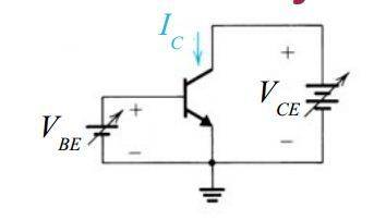
Circuit schematic of an NPN transistor with emitter grounded, a variable battery marked VBE between base and ground, and a variable battery marked VCE between collector and ground, with collector current IC labelled and an arrow showing its direction.

In textbooks, I usually see the circuit used to make Ic -Vce characteristics.
I see that there are no resistors at base and collector/emitter.
What will happen if VBE is larger than 1V or more?
Is the PN juction will break down?
How about if the transistor in saturation? Then if this is ideal transistor Vce = 0 but it is also connected to a external battery VBE ≠ 0. I am totally confused. Please help.
 
Attachments
  • Circuit schematic of an NPN transistor with emitter grounded, a variable battery VBE on the base and a variable battery VCE on the collector, with collector current IC marked by an arrow.
    Transistor.JPG
    5.3 KB · Views: 1,027
anhnha said:
Hi, this is not a homework. I need your help to understand basic concepts. I am learning by myself.
Circuit schematic of an NPN transistor with a voltage source VBE across base and emitter, a voltage source VCE across collector and emitter, collector current IC marked, and the emitter grounded; no meters or resistors shown.

In textbooks, I usually see the circuit used to make Ic -Vce characteristics.
I see that there are no resistors at base and collector/emitter.
What will happen if VBE is larger than 1V or more?
Is the PN juction will break down?
How about if the transistor in saturation? Then if this is ideal transistor Vce = 0 but it is also connected to a external battery VBE ≠ 0. I am totally confused. Please help.

That is not a real circuit to measure transistor characteristics. In a real one, there are meters (voltmeters and ammeters) and there are resistances. If nothing else, those of the bulk of the semiconductor and the wires.

Read http://www.electronic-factory.co.uk/transistor-operation/ and http://www.electronic-factory.co.uk/transistor-characteristics/, for example.

ehild
 
Thanks,
can you answer my questions with the circuit above? I am confused.
What will happen if VBE is larger than 1V or more?
Is the PN juction will break down?
How about if the transistor in saturation? Then if this is ideal transistor Vce = 0 but it is also connected to a external battery VBE ≠ 0.
 
  • Like
Likes   Reactions: 1 person
Are you sure you study from a proper book?
Yes, but the image above is in a lecture slide I got from the net.
Here is a set up in the lecture to illustrate early effect:
Slide titled Early Effect showing an ideal NPN BJT circuit with variable VBE and VCE sources and the graph of IC against VCE for VBE1 to VBE4, plus a mode table of VBE and VBC signs for each operating region.

In this circuit both Vbe and Vce can be changed.
What is the limits that I can apply for Vbe and Vce that don't break down the transistor?
For example, Vbe has to be in 0- 5V?
 
Attachments
  • Lecture slide titled Early Effect showing an ideal NPN BJT circuit with VBE and VCE sources and a graph of Ic against VCE for VBE1 to VBE4, plus a table of transistor operating modes.
    Early effect.JPG
    35.4 KB · Views: 1,144
The path Base->Emitter behaves like a forward biased diode.

The emitter is connected to 0V so the base voltage will be limited to roughly 0.7V. If you try and force it higher the transistor might well be damaged by excess current.

Graph of base current IB in microamps against base-emitter voltage VBE in volts for three curves labelled VCE = 1V, 10V and 20V, rising sharply above about 0.6V.


Personally I don't like the drawing you posted. You can control a transistor by varying the base voltage BUT it's much better to think of a transistor as a current controlled device. eg It's the base Current contols the Collector->Emitter Current.

This is because Vbe is temperature sensitive. If you try and control the base voltage the circuit can become temperature sensitive.

See this diagram which looks nearly identical but note the curves are labeled Ib rather than Vbe.

Graph of collector current IC in mA against collector-emitter voltage VCE in volts, with five curves labelled Ib = 50, 100, 150, 200 and 250 µA, rising steeply then flattening.
 
  • Like
Likes   Reactions: 1 person