Why Do Energy Bands Split and Merge in Semiconductors?

Join the discussion
Ask a follow-up here, or get your own question answered by working scientists, mathematicians and engineers — people, not an autocomplete.
Real named experts · corrections over time · the nuance an AI answer skips
1 reply · 13K views
hardyivan007
Messages
7
Reaction score
0
I was taught this in school but my teacher could not explain why the band splits again with decreasing atomic distance. Also, then i wondered how do you explain the fact the it splits again nicely into 4N states for the valence band and 4N states for the conduction band? Could some one help?
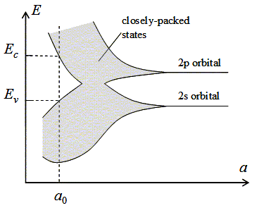
fig2_3_2.gif

Isolated carbon atoms contain six electrons, which occupy the 1s, 2s and 2p orbital in pairs. The energy of an electron occupying the 2s and 2p orbital is indicated on the figure. The energy of the 1s orbital is not shown. As the lattice constant is reduced, there is an overlap of the electron wavefunctions occupying adjacent atoms. This leads to a splitting of the energy levels consistent with the Pauli exclusion principle. The splitting results in an energy band containing 2N states in the 2s band and 6N states in the 2p band, where N is the number of atoms in the crystal. A further reduction of the lattice constant causes the 2s and 2p energy bands to merge and split again into two bands containing 4N states each. At zero Kelvin, the lower band is completely filled with electrons and labeled as the valence band. The upper band is empty and labeled as the conduction band.

Also, how would one redraw the above energy band diagram if the semiconductor was doped to become a n-type or a p-type?

Hope someone could help! Thank You!
 
Last edited:
Physics news on Phys.org
This diagram holds for all group IV elements in their diamond FCC crystal structure. Taking carbon as an example, isolated carbon atoms (far right of diagram) have discrete 2s and 2p levels. As you move to the left, the individual carbon atoms begin interacting with one another, which causes the energy levels to split into various combinations of the orbitals, creating the 2s and 2p bands with a certain bandwidth.

As you continue moving the carbon atoms closer, the bands ultimately overlap to form a metallic electronic structure. This is what happens in tin and lead: their lattice constant is larger than carbon, silicon, and germanium (because the atoms themselves are larger), but the structure is the same, so their valence s and p bands overlap to give a metal.

As you continue to move to the left, it becomes energetically favorable for the 4 valence electrons of each atom to pair up with 1 valence electron from each of their 4 nearest neighbors to “complete the octet.” This splits the band again, but this time, it’s most favorable for the 4 valence electrons to be equivalent (because the directions of the tetrahedron are equivalent), so the bands split into 4N “bonding” electrons and 4N “anti bonding” electrons. This is why the band gap for group IV elements increases from germanium to silicon to diamond.

This has certain practical implications: in the 90’s, a lot of research was poured into the electronic properties of strained silicon and other strained semiconductors to manipulate band gap and mobility. These materials eventually found their way into modern electronics.
 
Reply
  • Like
Likes   Reactions: nasu and Maarten Havinga