lamejane
- 11
- 2
- TL;DR
- Occurence of Voids after Annealing
Hello to all the experts out there!: )
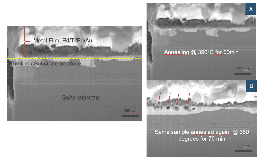
I have encountered a problem on my samples after Post deposition annealing [ Please refer to the crossectional SEM picture - B below].
Sample description : Thinfilm metal stack [ Pd/Ti/Pd/Au] deposited onto GaAs substrate using PVD
Post deposition annealing : Using a Hotplate exposed to clean room air
--> 60 min @ 390°C [ Picture A]
--> additionally 70 min @350°C on same sample B [ Picture B]
My Question to the Experts :
I see occurences of Voids at the thinfilm -Substrate interface [ see picture B] after annealing at 350°C for 70 min . What effect could explain this phenomenon ?
Is it due to an increase in tensile stress at the interface because of the high annealing temperature ? or is there a strong solid state diffusion of the metal atoms in the thinfilm leading to defects ?
The thinfilm metal stack contains : Pd/Ti/Pd/Au/15nm/30nm/30nm/250nm and is meant to serve as an Ohmic contact