How do SRAM and DRAM differ in terms of circuitry and data storage?

  • Thread starter Thread starter Wrichik Basu
  • Start date Start date
  • Tags Tags
    Cell Work
Click For Summary
SRAM and DRAM differ significantly in their circuitry and data storage methods. SRAM uses a configuration of transistors, specifically MOSFETs, to create stable states for data storage, relying on positive feedback mechanisms for retaining information. In contrast, DRAM utilizes capacitors to store charge, with the logical state determined by whether the charge is present or absent, necessitating periodic refresh cycles due to charge leakage. The discussion highlights that while SRAM is generally faster and consumes more power, DRAM can be less efficient for storing single bits due to its overhead requirements. Understanding these differences is crucial for applications in computer architecture and memory design.
Wrichik Basu
Science Advisor
Insights Author
Gold Member
Messages
2,180
Reaction score
2,721
TL;DR
How does a cell of SRAM work?
Summary: How does a cell of SRAM work?

I have computer science minor, and we have been given the task of finding out the differences between SRAM and DRAM. Simple enough? I thought so, until I got into the circuitry of a SRAM cell and got interested in finding how it works for storing, reading and writing data. Unfortunately I could not find a good website that explains this properly.

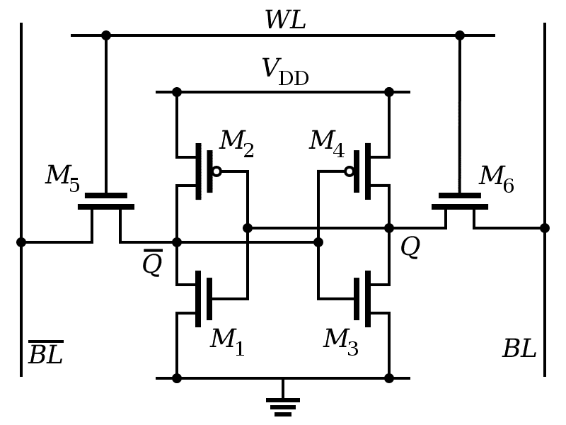
The diagram, taken from Wikipedia, is this one:
1567950522747.png

From Quora, M5 and M6 are access transistors, M2 and M4 pull up, M1 and M3 are pull down transistors. WL is probably a "word line" (read from somewhere else) which has to be high to allow a read and write operation.

On reading the explanation at Wikipedia, I have the following questions:

1. The M# are transistors, but why have they been drawn like that? We learned to draw transistors in a different way, isn't it?

2. Wikipedia states in the reading section,
In theory, reading only requires asserting the word line WL and reading the SRAM cell state by a single access transistor and bit line, e.g. M6, BL. However, bit lines are relatively long and have large parasitic capacitance. To speed up reading, a more complex process is used in practice: The read cycle is started by precharging both bit lines BL and BL, to high (logic 1) voltage. Then asserting the word line WL enables both the access transistors M5 and M6, which causes one bit line BL voltage to slightly drop. Then the BL and BL lines will have a small voltage difference between them. A sense amplifier will sense which line has the higher voltage and thus determine whether there was 1 or 0 stored.
Why will the voltage difference come?
 
Last edited:
Engineering news on Phys.org
Wrichik Basu said:
Summary: How does a cell of SRAM work?

1. The M# are transistors, but why have they been drawn like that? We learned to draw transistors in a different way, isn't it?
They are MOSFETs. P-channel and N-channel FETs. Do you have a guess why FETs are used for high-density RAM ICs instead of Bipolar transistors? :smile:
 
  • Like
Likes sophiecentaur
Wrichik Basu said:
Summary: How does a cell of SRAM work?

Summary: How does a cell of SRAM work?

I have computer science minor, and we have been given the task of finding out the differences between SRAM and DRAM. Simple enough? I thought so, until I got into the circuitry of a SRAM cell and got interested in finding how it works for storing, reading and writing data. Unfortunately I could not find a good website that explains this properly.

The diagram, taken from Wikipedia, is this one:


From Quora, M5 and M6 are access transistors, M2 and M4 pull up, M1 and M3 are pull down transistors. WL is probably a "word line" (read from somewhere else) which has to be high to allow a read and write operation.

On reading the explanation at Wikipedia, I have the following questions:

1. The M# are transistors, but why have they been drawn like that? We learned to draw transistors in a different way, isn't it?

2. Wikipedia states in the reading section, Why will the voltage difference come?


As the video mentioned, SRAM requires at minimum 4 transistors, and operates via the Boolean Method. Recommend investigating a bit more on the Boolean Method to understand that wiki diagram!
 
  • Like
Likes davenn
berkeman said:
They are MOSFETs. P-channel and N-channel FETs.
I thought so.
berkeman said:
Do you have a guess why FETs are used for high-density RAM ICs instead of Bipolar transistors?
Although I don't have too much knowledge on FETs, I believe the fact that FETs are voltage controlled rather than current controlled makes them superior to BJTs. Current-controlled biasing means more power consumption.
 
  • Like
Likes Asymptotic, davenn and berkeman
Wrichik Basu said:
Unfortunately I could not find a good website that explains this properly.
Here's a PDF from Signetics ( Philips Semiconductors, now, NXP Semiconductors N.V. )

It's probably not a good website that explains this stuff properly improperly, although

it does have pictures diagrams. . .

Signetics 25120-bw.pdf
Wrichik Basu said:
Simple enough? I thought so. . .
If that PDF makes things even more not simple, I have provided, at no obligation, a link

that will make you seem a genius in your computer science minor. . . maybe even,

giving you the opportunity to publish?. . . 🎓 .💰The genius link I promised is. . . HERE

.
 
Last edited:
Wrichik Basu said:
Why will the voltage difference come?

The 4 transistors, M1,M2,M3,M4 can be in two stable states, one where Q is high and Qbar is low, and one where Qbar is high and Q is low. If Q is high and Qbar is low, then M1 is on and M3 is off. When the WL is pulled high, both M1 and M5 are on, so current will flow from BLbar through M5 and M1, pulling BLbar down. Since M3 is off, no current will flow through M6 and M3, so the voltage on BL does not change. So a voltage difference develops between BL and BLbar, with the voltage on BL staying high and the voltage on BLbar dropping. In the opposite state, BLbar stays high, and BL drops. Does this make sense?
 
  • Informative
Likes Wrichik Basu
phyzguy said:
Does this make sense?
Yes, thanks for the explanation. One question: you explained this with M1 and M3, without using M2 and M4. How are the latter useful in the circuit?
 
Wrichik Basu said:
Yes, thanks for the explanation. One question: you explained this with M1 and M3, without using M2 and M4. How are the latter useful in the circuit?
M2 and M4 don't take part in the reading operation. Their purpose is to maintain the two stable states. Take the case when Q is high and Qbar is low. Then M3 is off. When not reading, WL is low, so M5 and M6 are off. Then there is nothing to hold Q high, so over time the charge on Q will gradually leak away. But when Qbar is low, M4 is on, so it holds node Q high. This is why it is a static RAM, because it will hold information indefinitely, as long as power is supplied.
 
  • Like
Likes Asymptotic and Wrichik Basu
While describing the write process, Wikipedia states,
This works because the bit line input-drivers are designed to be much stronger than the relatively weak transistors in the cell itself so they can easily override the previous state of the cross-coupled inverters. In practice, access NMOS transistors M5 and M6 have to be stronger than either bottom NMOS (M1, M3) or top PMOS (M2, M4) transistors. This is easily obtained as PMOS transistors are much weaker than NMOS when same sized.
In what sense are the PMOS weaker than NMOS?
 
  • #10
Wrichik Basu said:
While describing the write process, Wikipedia states, In what sense are the PMOS weaker than NMOS?
Look at the equation for the MOSFET current:

{\displaystyle I_{\text{D}}=\mu _{n}C_{\text{ox}}{\frac {W}{L}}\left(\left(V_{\text{GS}}-V_{\rm {th}}\right)V_{\text{DS}}-{\frac {{V_{\text{DS}}}^{2}}{2}}\right)}


The μ term is the carrier mobility. In silicon, the hole mobility is about 1/3 of the electron mobility, so all else being equal, the PMOS are much weaker. As for the NMOS, the SRAM cell is usually designed so M5 and M6 have wider W than M1 and M3.
 
  • Like
Likes Wrichik Basu
  • #11
Wrichik, I suspect the question asker is looking for a higher-level answer as there are a large number of possible SRAM and DRAM circuit topologies all with various implementation trade-offs. I don't think they want you to analyze that particular example of a circuit.

I suspect what they want is you to note that most (all?) SRAM topologies are latch based which means they store data via a positive feedback mechanism. See the following link [1] but especially this section, "How can we make a circuit out of gates that is not combinatorial? The answer is feedback, which means that we create loops in the circuit diagrams so that output values depend, indirectly, on themselves. If such feedback is positive then the circuit tends to have stable states, and if it is negative the circuit will tend to oscillate.". So latches (and therefore SRAM) written and read via normal combinatorial logic, and the state is stored via positive feedback.

DRAM is based off a capacitor which is a device that literally stores charge. In rough terms the logical state stored on the cell is equivalent to the boolean statement, is the charge inside the capacitor presently non-zero. Here the state is written by adding or removing the charge from the capacitor, it is stored by the physics of the device, and it is read by attempting to transfer that charge to a downstream circuit. DRAM has a ton of implementation details (like the capacitor leaks charge and needs to be replenished from time to time if one wants to retain the non-zero logical state) but that's the gist.

One other quick point: You'll often see statements like DRAM is slower but lower power than SRAM, etc. Although these statements are true for the typical case they are not strictly true. For example, DRAM comes with a lot of overhead (i.e. the circuit that replenishes from time to time) so if one only wants to store 1 bit, DRAM can be very high power compared to SRAM.

[1] https://www.labri.fr/perso/strandh/Teaching/AMP/Common/Strandh-Tutorial/flip-flops.html
 
  • Informative
Likes Tom.G and anorlunda

Similar threads

  • · Replies 14 ·
Replies
14
Views
5K
  • · Replies 1 ·
Replies
1
Views
4K
Replies
7
Views
2K