SUMMARY
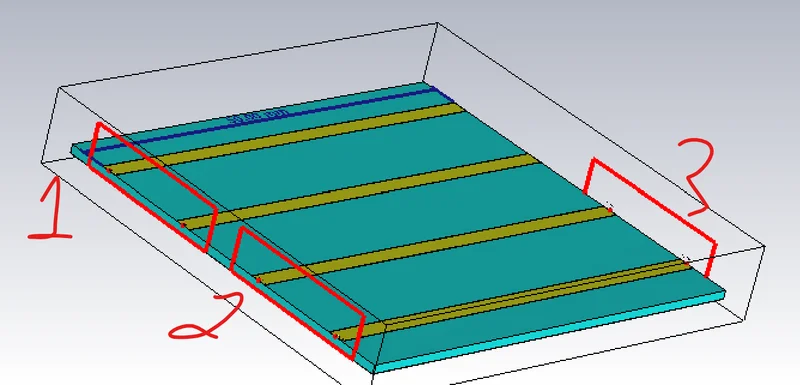
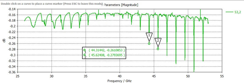
The discussion focuses on interpreting Far-End Crosstalk (FEXT) and Near-End Crosstalk (NEXT) resonance patterns in PCB differential pair simulations. The user simulated three differential lines with substrate dielectric constant (εr) of 4.1 and trace lengths of 50mm, observing resonances spaced by 1.23 GHz in the SDD23 parameter. The key question addresses correlating resonance frequency spacing to the physical aggressor trace length, confirming that resonance spacing directly relates to the electrical length of the aggressor trace and substrate properties. This establishes a method to extract trace geometry information from crosstalk resonance patterns in high-speed PCB design.
PREREQUISITES
- Understanding of S-parameters, specifically SDD23 in differential signaling
- Knowledge of PCB transmission line theory and differential pair design
- Familiarity with crosstalk phenomena: Far-End Crosstalk (FEXT) and Near-End Crosstalk (NEXT)
- Dielectric constant (εr) impact on signal propagation and resonance frequency calculation
NEXT STEPS
- Study calculation of resonance frequencies from trace length and dielectric constant
- Analyze S-parameter simulation tools for differential pair crosstalk (e.g., Keysight ADS, Ansys HFSS)
- Explore PCB trace impedance modeling and its effect on crosstalk patterns
- Investigate methods to extract physical trace geometry from frequency domain measurements
USEFUL FOR
PCB designers, signal integrity engineers, and RF simulation specialists working on high-speed differential pair layout and crosstalk mitigation in multilayer PCB designs.