James_AA
- 1
- 0
- TL;DR
- An optical experiment is proposed to validate points
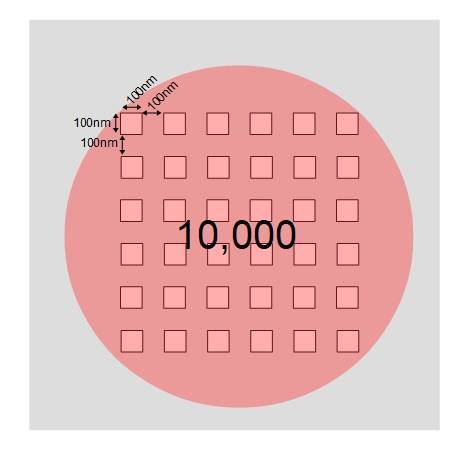
Hi everyone, let me propose an experiment to see if you agree with my points. There is a 1cm2 1-micron thick aluminum substrate with a matrix of 100x100 nano-holes each with 100x100nanometers cross section separated by 100nanometers. Then, we focus a 1W laser with visible wavelength:

1- UNDETECTABLE:
The matrix of nan-holes is equivalent to a square of 10,000x10,000nm which is a surface of 1E08nm2 = 1E-010m2
The 1W laser produces 1J per second which is 1 kg⋅m2⋅s−3 in the calculated surface of 1E-010m2 equals to 1E-010J= 0.1 nanowatts.
So, even assuming total transmission, such 0.1 nanowatts are undetectable by conventional high sensitivity optical power sensors (normally, 10nW minimum detectable power).
2-ALTERANTIVE:
A 5W laser is used for non-industrial laser cutting so to avoid burning the 1-micron substrate, 1W was chosen. However, even increasing the power to 4W would still make it undetectable. A solution could be using a 100W high power LED plus some lenses. Or even the following 1,500W LED:
[Spammy link deleted by the Mentors]
3-POINTLESS:
Being nano-holes at the subwavelength scale of light, no optical transmission is posible.
So, thanks for reading and let me know your thoughts.
Last edited by a moderator: