arhzz
- 284
- 58
- Homework Statement
- -
- Relevant Equations
- -
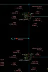
Hello; I am trying to build a Gm cell using a degenerated differential pair; I also have a Common Feedback Circuit so that I can keep the output at Vdd/2; This is how my Gm Cell looks like

Basically I have M1 and M2 Nmos and i feed it a differential voltage, the bottom transistors are a part of a current mirror that is being biased (and that works I have checked it) ; at the top are diode connected PMOS as loads (M3 and M4) and than I have a push pull stage; M13 is part of a enable circuit and can be disregarded. (the red things around the transitors are small signal parameters I didnt show them so its easier to see the schematic)
Now this is my test bench

I have a block that converts a single to differential voltage and feed it to the Gm; also the biasing is here done via an ideal current source and the CMFB and CMFB_ideal blocks are used to create 0.75 (so Vdd/2) at vop and von; for that purpose I also have the 2 large resistors and the 0V sources are only there so that I can measure the current; The CMFB block is working as intented since the voltages vop and von are 0.76 and my goal is to have them at 0.75
Now as you can see I am biasing it with 2.3u and I am expecting that at my Iop and Ion; but this is what I get at Iop

I get something in nA; Now I am genuinly confused why this is the case;
I plotted the currents in the 2 Transistors in my Gm2 block that are connected to IOP (M16 and M18) and this is how they look like

A little bit more than 2.3uA but still nowhere near nA; Can anyone maybe try and guide me through how I can figure out where this is going wrong?
Thanks in advance
Basically I have M1 and M2 Nmos and i feed it a differential voltage, the bottom transistors are a part of a current mirror that is being biased (and that works I have checked it) ; at the top are diode connected PMOS as loads (M3 and M4) and than I have a push pull stage; M13 is part of a enable circuit and can be disregarded. (the red things around the transitors are small signal parameters I didnt show them so its easier to see the schematic)
Now this is my test bench
I have a block that converts a single to differential voltage and feed it to the Gm; also the biasing is here done via an ideal current source and the CMFB and CMFB_ideal blocks are used to create 0.75 (so Vdd/2) at vop and von; for that purpose I also have the 2 large resistors and the 0V sources are only there so that I can measure the current; The CMFB block is working as intented since the voltages vop and von are 0.76 and my goal is to have them at 0.75
Now as you can see I am biasing it with 2.3u and I am expecting that at my Iop and Ion; but this is what I get at Iop
I get something in nA; Now I am genuinly confused why this is the case;
I plotted the currents in the 2 Transistors in my Gm2 block that are connected to IOP (M16 and M18) and this is how they look like
A little bit more than 2.3uA but still nowhere near nA; Can anyone maybe try and guide me through how I can figure out where this is going wrong?
Thanks in advance