Interpreting VIA PCB through TDR and TRT

  • Thread starter Thread starter yefj
  • Start date Start date
yefj
Messages
64
Reaction score
2
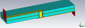
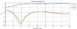
Hello ,I have simulated a basic VIA (shown in the photo) in CST EM simulator from 0 to 40GHz and extracted its attached S2P.
using the code below I resampled it and made IFFT with multiplied the normalised hamming window.
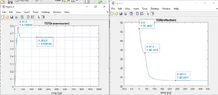
I got the following plots in MATLAB.
Is there a way to interpret the VIA properties threw these TRT and TDR plots?
Thanks.
Code:
clear all
Sp = sparameters('via.s2p');
Sp.Parameters(1,1,1)=0;
freqs=Sp.Frequencies; %40000X1
s11_half=Sp.Parameters(1,1,:);
s21_half=Sp.Parameters(2,1,:);
if freqs(1) ~= 0
           s11_dc = interp1(freqs, s11, 0, 'linear', 'extrap');
end

left_side=squeeze(s11_half);
left_side_s21=squeeze(s21_half);

% ===== Resample to uniform frequency grid =====
fi = linspace(freqs(1), freqs(end), length(freqs)).'; %40000X1
s11_resamples = interp1(freqs, left_side, fi, 'linear');
s21_resamples = interp1(freqs, left_side_s21, fi, 'linear');
right_side_miror=conj(s11_resamples(end-1:-1:2));
right_side_miror_s21=conj(s21_resamples(end-1:-1:2));
s11_full=[ s11_resamples;right_side_miror];
s21_full=[ s21_resamples;right_side_miror_s21]; %%


w = ifftshift(hamming(length(s11_full),'periodic'));
w=w./max(w);

%%%%%%%%%%%%%
df = fi(2) - fi(1);
N = length(s11_full);
t = (0:N-1).' / (N * df);   % time axis

rho = cumsum(real(ifft(s11_full.*w)));
z = (1+rho)./(1-rho)*50;

figure;
plot(t*1e12, z);
xlim([-100 450]);
xlabel('time [ps]');
title('TDR(reflection)');


figure;
plot(t*1e12, cumsum(real(ifft(s21_full.*w))));
grid on; grid minor; set (gca, 'gridalpha', 0.2); set(gca, 'minorgridalpha', 0.05);
xlim([0 1000]);
xlabel('time [ps]');
title('TDT(transmission)');
 

Attachments

  • Capture.webp
    Capture.webp
    19.9 KB · Views: 1
  • 3D_shape.webp
    3D_shape.webp
    20.2 KB · Views: 1
  • S_param.webp
    S_param.webp
    21.5 KB · Views: 1
Engineering news on Phys.org
Hello , I have resimulated the structure in another way and got a result much better to realistic DC value
s-parameters .
I made again IFFT to the S2p file and got the attached plots.

given my situation few questions:
1.given my 40GHz BW what kind of sizes I can use TDR TRT effectively
2.given my new IFFT plots is how can I see the geometrical properties of the VIA in them?
Is there some intuitions?

1775217703687.webp

1775217723603.webp

1775217749061.webp
 
yefj said:
Is there a way to interpret the VIA properties threw these TRT and TDR plots?
You have two tracks with known impedance, joined through the PCB by a short cylindrical via. The via will probably not match the impedance of the tracks, so it will appear to be a quarter wave transformer with the via length, adjusted for velocity factor √Er.

Usually, only ground and power are routed through vias, and then through multiple parallel vias. It is not good practice to run signals through vias, at microwave frequencies. Keep signals in the signal plane, between or above ground plane(s).

My guess is that the via will appear to be a short cylindrical transmission line, probably inductive. You should be able to see the length of the via in the wavelength of the highest transmission frequency, and the impedance of the via in the TDR. Thinner vias are more inductive, so you may be able to adjust the via diameter until it matches the track impedance on both sides of the PCB. Feathering the track as it approaches the via, may ease reflection from the transition. To get a first approximation, compute the impedance of the via as a longer cylindrical transmission line.
 
  • Like
Likes   Reactions: berkeman
yefj said:
I have simulated a basic VIA (shown in the photo)
1775251601608.webp


What you show is a 3-layer PCB, which is not used in practice.

Baluncore said:
It is not good practice to run signals through vias, at microwave frequencies. Keep signals in the signal plane, between or above ground plane(s).
This point made by @Baluncore should be emphasized. It is generally a design error to run high-frequency signals through vias, since the resulting ##Z_0## is not constant and does not match the transmission line. The transmission line physical structure and resulting ##Z_0## need to be maintained throughout the length of the TL from the transmit gate to the receive gate(s). Also, the TL must be properly terminated to avoid ringing (either forward-terminated for point-to-point TLs with a single receive gate, or back-terminated for TLs that have several receive gates).

Back in the early days of the FCC imposing EMI limits on electronic devices (like in the mid-1980s), one of the biggest problems in quieting down digital PCBAs was that little attention was paid to the routing of fast digital traces, and the resulting ringing from all the ##Z_0## mismatches caused lots of unintentional radiation from the PCBAs and the product enclosures and cables. [1]

Note also that this constant ##Z_0## requirement means that the TL signal trace should not pass close to other traces or grounded features, since this can also alter the ##Z_0## value.

[1] High Speed Digital Design, A Handbook of Black Magic, by Howard W. Johnson and Martin Graham, Chapter 7 on Vias, PTR Prentice Hall, 1993.
 
Last edited:
  • Like
Likes   Reactions: Baluncore

Similar threads

  • · Replies 1 ·
Replies
1
Views
1K
Replies
2
Views
2K
  • · Replies 5 ·
Replies
5
Views
6K
  • · Replies 1 ·
Replies
1
Views
2K
Replies
5
Views
8K
  • · Replies 1 ·
Replies
1
Views
4K
  • · Replies 3 ·
Replies
3
Views
4K