High-Power LEDs -- Maximum 'Lumen-Density'?

  • Thread starter Thread starter Solid-Statist
  • Start date Start date
  • Tags Tags
    Leds Maximum
Click For Summary

Discussion Overview

The discussion revolves around the maximum density of high-power LED arrays that can be fabricated on a semiconductor wafer, focusing on metrics such as lumens output or watts consumed per area. Participants explore theoretical limits, practical considerations, and the implications of different semiconductor materials.

Discussion Character

  • Exploratory
  • Technical explanation
  • Debate/contested
  • Mathematical reasoning

Main Points Raised

  • Some participants question the feasibility of the original inquiry due to heat management issues, suggesting that no LED die would be designed to fail under extreme conditions.
  • Others propose rephrasing the question to consider scenarios where effective cooling, such as liquid nitrogen, is applied to maintain the LED die temperature below maximum limits.
  • One participant suggests determining maximum density by examining the dimensions of typical high-power LED dies and the scribe lines used in wafer fabrication.
  • Another participant provides a specific example of a high-power LED die, mentioning dimensions and power ratings, and discusses estimating die size based on available datasheets.
  • There is mention of low-power LEDs and their differences from high-power LEDs in terms of lumen and power density, highlighting design variations such as multi-junction configurations.

Areas of Agreement / Disagreement

Participants express differing views on the initial question's validity and feasibility, with some agreeing on the need for cooling considerations while others remain skeptical about the practicality of the inquiry. The discussion does not reach a consensus on the maximum density achievable.

Contextual Notes

Participants note limitations related to assumptions about cooling methods and the specific semiconductor materials used, as well as the need for more information on typical die dimensions and power ratings.

Who May Find This Useful

This discussion may be of interest to those involved in semiconductor fabrication, LED technology development, and thermal management in high-power lighting applications.

Solid-Statist
Messages
12
Reaction score
5
TL;DR
On a LED semiconductor wafer, what is the maximum density of 'light production' per area?
Does the semiconductor substrate matter in maximizing density?
Light-emitting diodes (LEDs) are replacing traditional lighting technology -- such as halogen -- in high-power lamps, as LEDs are much more efficient (Lumens/W) and longer-lasting.

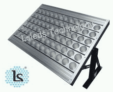
A commercial example of high-power LED flood lights: High Power 3000W LED Flood Light - Lsleds
1654623262149.png
NOTE: The above Chinese unit has an array has 72 lamps, so each lamp's LED semiconductor(s) consume about 42W, which translates to as much as 8000 lumens from a single lamp.​

QUESTIONS:

What is the maximum density of high-power LED arrays that can be printed on a semiconductor wafer, with the metrics of Lumens-output or Watts-consumed per area? (This is independent of packaging the semiconductors into a subassembly and considerations of cooling during operation.)

Is maximum density of high-power LED arrays a function of semiconductor type? (Si, SiC, GaAs, Sapphire, etc)
 
Engineering news on Phys.org
I believe this is an ill-considered question. Heat will always be the issue and no one will design an LED die which will melt in milliseconds.
 
hutchphd said:
I believe this is an ill-considered question. Heat will always be the issue and no one will design an LED die which will melt in milliseconds.
No doubt that would be true with conventional LED packaging.

This was just a theoretical question. Perhaps if it's rephrased...

Assuming that you have a tank of liquid nitrogen (or cooling equiv) to keep the LED die temp at/below its maximum limit ... what is the maximum density of high-power LED arrays that can be printed on a semiconductor wafer, with the metrics of Lumens-output or Watts-consumed per area?
 
Solid-Statist said:
what is the maximum density of high-power LED arrays that can be printed on a semiconductor wafer, with the metrics of Lumens-output or Watts-consumed per area?
It may be easiest just to find out what a typical high power LED die's dimensions are, since the scribe lines to break the wafer into die will be small compared to the die dimensions. Will that give you what you need? Do you know the typical die dimensions for some high power LED die that you are looking at?

I'll page @nsaspook since this question is right in the middle of his wheelhouse.

Also, I did a Google search on high power led fabrication wafer and got some pretty good hits. Here are a couple of them in case they help:

https://www.planetanalog.com/led-single-die-solutions-for-high-power-products/

https://www.universitywafer.com/silicon-based-gan-led-wafer.html
 
  • Like
  • Informative
Likes   Reactions: hutchphd, dlgoff, Solid-Statist and 1 other person
berkeman said:
It may be easiest just to find out what a typical high power LED die's dimensions are, since the scribe lines to break the wafer into die will be small compared to the die dimensions. Will that give you what you need? Do you know the typical die dimensions for some high power LED die that you are looking at?
Yes, that methodology would work great to determine the state-of-the-art 'maximum lumen density' of LED technology. I don't (yet) know much about existing "typical die dimensions for some high power LED die", but know what to ask. Perhaps if I re-rephrase the questions:

In high-power LED subassemblies that you may be familiar with, what is the semiconductor-die dimension and its lumen/wattage-rating? What semiconductor substrate is used?

Also, nice googling skills. Great article on 'single-die solutions', learned a lot ... thanks so much!
 
  • Like
Likes   Reactions: hutchphd and berkeman
Solid-Statist said:
I don't (yet) know much about existing "typical die dimensions for some high power LED die", but know what to ask.

I think you can get a reasonable estimate of the die size from this figure from the first link that I posted to the Plessey power LED information:

1654629225275.png


...and the datasheet info for their 7070 series LED that the article talks about. It looks like the base is 7mmX7mm, so if you assume that the drawing above is to scale, that will let you estimate the dimensions of that die. Datasheet info found here:

https://uk.rs-online.com/web/p/leds/1696969
 
  • Like
Likes   Reactions: Solid-Statist
berkeman said:
It looks like the base is 7mmX7mm, so if you assume that the drawing above is to scale, that will let you estimate the dimensions of that die.

Let’s give this a shot…
1654621667297.png


In the drawing, the high-power LED die is about 1/5th the length of the 7x7mm package, so the die length would be 1.4mm and its area about 2mm^2.

The Plessey datasheet notes a power level of up to 15W for the device, so that would mean the maximum thermal load on the die could reach 7.5 W/mm^2, or over 4800 W/sqin. Does that sound right?
 
hutchphd said:
Here's some low-power small ones :
https://www.i-micronews.com/wafer-level-micro-led-matrix-delivers-high-brightness-at-2540dpi/
The Plessey mentioned by @berkeman is likely a multi-junction die (probably 3 in series} so slightly different in design. The devil is in the detail.

From a relative standpoint, how much do "low-power" LEDs differ from high-power LEDs in their maximum lumen- or power-density?

The Plessey paper on LED Single-Die Solutions notes that this configuration has an advantage over "multi-junction die" in that there is no dimming or shadowing in the light output at the gaps between dies (see below).

1654622801780.png
 

Similar threads

  • · Replies 15 ·
Replies
15
Views
3K
Replies
2
Views
2K
  • · Replies 2 ·
Replies
2
Views
3K