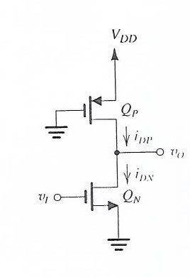
How does the Pseudo NMOS inverter use Qp as an active load?

  • Thread starter Thread starter janor
  • Start date Start date
  • Tags Tags
    Inverter
Click For Summary
SUMMARY

The discussion centers on the operation of the Pseudo NMOS inverter, specifically how Qp functions as an active load. Participants clarify that Qp, biased at -5V, acts as a current source rather than a short circuit, influencing the output voltage based on the relative strength of Qn and Qp. The conversation highlights the importance of using proper biasing techniques, such as degeneration resistors, to ensure stable operation and accurate current sourcing in both discrete and integrated circuits. Additionally, the use of feedback circuits for voltage generation is emphasized as a best practice in circuit design.

PREREQUISITES
  • Understanding of NMOS transistor operation and biasing techniques
  • Familiarity with circuit simulation tools like Multisim
  • Knowledge of current source design and feedback mechanisms
  • Experience with integrated circuit design principles
NEXT STEPS
  • Research NMOS transistor biasing techniques, including degeneration resistors
  • Explore current mirror design in integrated circuits
  • Learn about feedback circuits for voltage regulation in analog designs
  • Investigate the effects of temperature and doping variations on transistor performance
USEFUL FOR

Electrical engineers, circuit designers, and students studying integrated circuit design who seek to deepen their understanding of NMOS inverter configurations and active load implementations.

janor
Messages
3
Reaction score
0
Hi

in the Pseudo NMOS inverter below
attachment.php?attachmentid=38326&stc=1&d=1314474465.jpg


I don't understand how Qp acts as an active load, what I understand is that with this configuration Qp's Vgs is -5V which means that this transistor is always on (short circuit), now if the input to the circuit is low this means that Qn is off but Qp is on so the output will be high, but if the input is high this means that both Qn & Qp are on, now how come the output will be low? Shouldn't it be floating?

and I tried a simulation on Multisim and the results was as I expected, when the input was low the output was 5V, and when the input was high the output was 4.6V.
 

Attachments

  • Untitled.jpg
    Untitled.jpg
    6.6 KB · Views: 2,530
Engineering news on Phys.org
Yes, it does seem to be wrong.

I found a similar circuit:
images?q=tbn:ANd9GcTX2U5LTSUGTZxdUPvcdr8_TGje7EmG7fQM2DmdJ69Apr2QoWGP.png


but both gates on this are joined together and driven with a rail to rail digital signal.

Cascode circuits like this one:
cascode-amplifier-circuit.jpg

have both FETs of the same polarity and the top one is biassed with a voltage divider. The output is taken from the top, too, instead of at the junction of the two devices.

It seems that you could have a similar voltage divider on the first circuit, so that the top FET behaves like a constant current generator. Then the output would vary according to the resistance of the lower FET.
 
It is wrong in so many level! You cannot bias the MOSFET without a source resistor to setup the current. V_{GS}\; varies a lot from transistor to transistor, you cannot set bias with a set voltage without degeneration resistors at the source. Also you cannot expect to set up a voltage using two constant current sources even if you set the two MOSFET up correctly as a constant current source. You are going to need negative feedback to set up a stable voltage. I designed plenty of MOSFET circuits and I know. With a circuit like this, even if you achieve constant current, it will stuck on one rail or the other because you cannot get the two current to be equal.
 
Last edited:
janor said:
I don't understand how Qp acts as an active load, what I understand is that with this configuration Qp's Vgs is -5V which means that this transistor is always on (short circuit)

No, not a short circuit, a current source. The trick is that the top (pullup) device has to be a lot weaker than the bottom (main switching) device. This is typically achieved by area (cross section) ratio matching.

and I tried a simulation on Multisim and the results was as I expected, when the input was low the output was 5V, and when the input was high the output was 4.6V.
See if multisim will allow you to alter the cross section area of the devices model (I know spice does). Set the relative area of the top device to 0.1 and repeat your simulation.
 
Last edited:
It is a bad practice to set up a current source with a set voltage like the schematic. Vgs vary widely even with same model. Temperature drift is severe. People do it inside integrate circuits as current mirror because you can make the two adjacent transistor very close in characteristics, you can even scale current by scaling the geometry of the two transistors in the integrated circuits. This is a very common method to get constant current sources in ICs. When I was designing ICs, I still use degenerating resistor for more precision circuits.

Only if AND only if it is in the same die close to each other and at same orientation you can set up current source like this. AND even at that, nobody with the right mind will set up a voltage using two constant current source like in the schematic inside an IC. Constant current source has very high output impedance, all it takes is the top and bottom are off by nano amps, the voltage will be stuck on one rail or the other.

In discrete transistors, this is a very very bad idea. You don't need simulation to tell you that. In discrete transistor, there is no way for you to know the difference in doping of the two separate die. Look at the data sheets, they only give you a range of the typical turn on characteristic. It can vary by a mile in individual device.
 
Hi yungman. I believe that the context here is integrated circuits. I can see little reason to try and build an inverter like that out of discrete components, and much better to just use a pullup resistor if you did.

If you go back to the 1980's nmos devices like the 8085 uP were built in their millions using a very similar configuration to that given by the OP (but with a depletion mode nmos device as that current source pull-up).
 
uart said:
Hi yungman. I believe that the context here is integrated circuits. I can see little reason to try and build an inverter like that out of discrete components, and much better to just use a pullup resistor if you did.

If you go back to the 1980's nmos devices like the 8085 uP were built in their millions using a very similar configuration to that given by the OP (but with a depletion mode nmos device as that current source pull-up).

Hi Uart

I did not assume it is integrated circuit. Even in integrate circuit it is not correct. Most of the case circuit looks like these:

145357[/ATTACH]"]
359gu4j.jpg


In Fig 2, a FET is used to set up a reference voltage and the voltage drive many other transistors with different geometry ratios to get different current. They might call it \;V_{bias}\;, but it is a compensated voltage with all the drift, dimension, doping considered in it. With this, it is perfectly legal and is a usual practice. This is nothing to do with putting a voltage to set up a constant in the straight sense. This is current mirror design. In Fig 2, I can get M times the Iref and N times Iref by scaling the dimension of the transistors.

We usually generate a voltage with a feedback circuit like in Fig 1 even in integrated circuits, not with just two current sources. As I explained before that even inside an integrated circuit, you cannot get this accurate to have it run in open loop.
 

Attachments

  • 359gu4j.jpg
    359gu4j.jpg
    3 KB · Views: 465
Last edited:
Hi yungman. Are you sure you're not confusing the digital logic device (not gate) of which the OP was inquiring with linear devices. Your circuits appear to be related to current mirror biasing of linear circuits.
 
Last edited:
uart said:
Hi yungman. Are you sure you're not confusing the digital logic device (not gate) of which the OP was inquiring with linear devices. You circuits appear to be related to current mirror biasing of linear circuits.

Yes, I went back to look at the op more, I assume it was linear, so Fig 1 don't apply, but Fig 2 still apply because you don't just use a straight voltage to set up a current source, it become unpredictable how much current is the current source and the IC would be very Vcc dependent. Say in digital logic, the Vcc is spec to use between 4.5 to 5.5V supply, this means the Vgs can vary 1V and that could be a huge current different. With constant current source like it Fig 2, you achieve Vcc independent...to a certain extend.

My experience in IC design was mostly in the early 80s and I mainly design linear ICs. Unless if the p FET is really designed as a constant current device that when the higher the \;V_{DS}, the narrow the channel and the higher the channel resistance which result in constant current.
 

Similar threads

Replies
6
Views
2K
  • · Replies 5 ·
Replies
5
Views
7K
Replies
5
Views
3K
  • · Replies 21 ·
Replies
21
Views
3K
  • · Replies 10 ·
Replies
10
Views
2K
  • · Replies 9 ·
Replies
9
Views
2K
  • · Replies 2 ·
Replies
2
Views
3K
  • · Replies 4 ·
Replies
4
Views
2K
  • · Replies 6 ·
Replies
6
Views
3K
Replies
53
Views
10K