LT spice result analysis, Capacitance Multiplier vs RC filter circuit

Click For Summary
SUMMARY

This discussion focuses on the simulation results of an RC filter circuit versus a Capacitance Multiplier (CM) circuit using LTspice. The results indicate that the output current (Iout) of the CM circuit is unexpectedly higher than that of the RC filter, contradicting the theoretical expectation that Iout (CM circuit) should be less than Iout (RC filter). Key findings include Vout and Iout measurements for both circuits, with the CM circuit showing a Vout (dc) of 0.323751 and Iout (dc) of 0.0323751, while the RC filter has a Vout (dc) of 0.0458716 and Iout (dc) of 0.00458716. The discussion also highlights potential issues in the simulation setup, such as the use of two voltage sources and the choice of transistor models.

PREREQUISITES
  • Understanding of LTspice simulation software
  • Knowledge of RC filter and Capacitance Multiplier circuit designs
  • Familiarity with output current (Iout) and voltage (Vout) measurements
  • Basic concepts of ripple voltage in power supply circuits
NEXT STEPS
  • Investigate the differences between the 2N4401 and 2N2222 transistor models in LTspice
  • Learn about the effects of load resistance on output current in capacitor circuits
  • Explore the significance of ripple voltage and its measurement techniques in power supply design
  • Study the impact of input waveform characteristics on circuit performance in LTspice simulations
USEFUL FOR

Electrical engineers, circuit designers, and students interested in power supply design and simulation using LTspice, particularly those analyzing the performance of RC filters and Capacitance Multiplier circuits.

brainbaby
Messages
232
Reaction score
5
Hi friends,

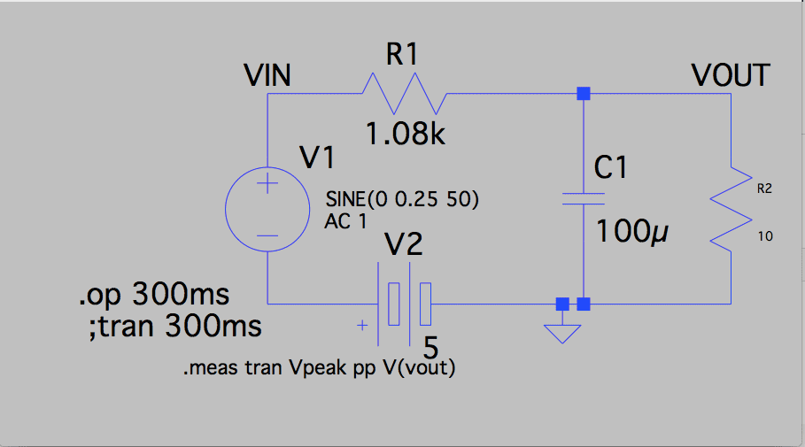
I have simulated two circuits, one is an RC filter and other is a Capacitance multiplier.
My aim of experiment is to validate a decrease in Iout (load current) of CM circuit as compared to load current in RC filter circuit.

Theoretically,
Iout (CM circuit) < Iout (RC filter)
Vp-p (CM circuit) < Vp-p (RC filter)

My results:
1.RC filter

Vout (dc) = 0.0458716 ( .op 300ms)
Iout (dc) = 0.00458716

Vout (ac) = 43.7 ~ 48 mV (.tran 300ms)
Iout (ac) = 4.80 ~ 4.37 mA

Vp-p (ripple) = 0.00437018 (.meas)

2.CM circuit


Vout (dc) = 0.323751
Iout (dc) = 0.0323751
Vout (ac) = 322 ~ 327 mV
Iout (ac) = 32.65 ~ 32.15 ma

Vp-p (ripple) = 0.00521016 (.meas)


From the above results its quite clear that implementing CM circuit causes Iout to increase which particularly against the aim of the CM circuit. As the CM circuit works by decreasing the load current which according to load POV can be visualised as increase in capacitance.
We can also see the peak to peak ripple voltage in both the circuits, Vp-p for CM circuit should be less than Vp-p ripple of an RC filter, but again the simulations results are quite opposite.

What's wrong here??
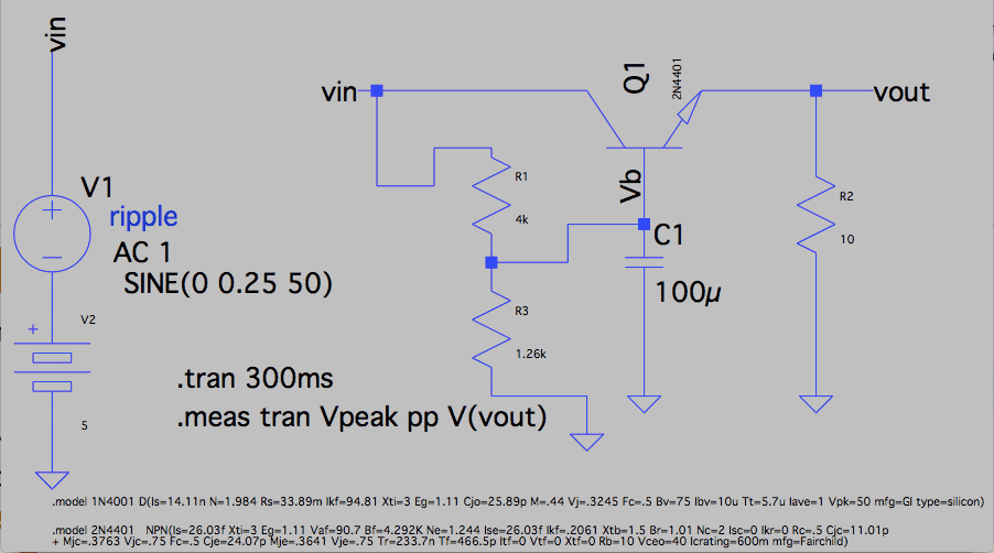
CM circuit.png


RC filter.png
 

Attachments

Engineering news on Phys.org
Is this not just an extension of your previous thread ?
https://www.physicsforums.com/threads/measuring-ripple-reduction-in-ltspice.1001493/

Why make it so complex ? You have too many places in the circuit to hide difficulties and differences. If the two circuits were merged into one_file.asc, you could compare the results directly.

1. Why specify two voltage sources in series when the DC offset can be specified in one ?

2. What is so special about the detailed 2N4401 model ? Why can you not use a traditional 2N2222 that is included in every version of LTspice ?

3. When 50 Hz is “full wave” rectified, the ripple approximates a saw-tooth with a fundamental frequency of 100 Hz. By specifying a 50 Hz sinewave, you are analysing a frequency component that does not exist, while ignoring every significant harmonic.
 
Because the CM circuit is buffered with the emitter follower, it has a higher output voltage and therefore a higher output current when operating into the same load resistance. The ripple in the CM circuit is also less because load current is not being drawn from the capacitor.

I have given the input waveform a 100 Hz saw-tooth.
Also, offset the DC of the CM voltage in the plot to get better resolution.

schematic-10.jpg

PlotOut-10.jpg
 

Attachments

Last edited:
Most likely this can only be answered by an "old timer". I am making measurements on an uA709 op amp (metal can). I would like to calculate the frequency rolloff curves (I can measure them). I assume the compensation is via the miller effect. To do the calculations I would need to know the gain of the transistors and the effective resistance seen at the compensation terminals, not including the values I put there. Anyone know those values?

Similar threads

  • · Replies 10 ·
Replies
10
Views
4K
  • · Replies 10 ·
Replies
10
Views
2K
  • · Replies 8 ·
Replies
8
Views
8K
  • · Replies 3 ·
Replies
3
Views
2K
Replies
3
Views
2K
  • · Replies 1 ·
Replies
1
Views
4K
  • · Replies 5 ·
Replies
5
Views
3K
  • · Replies 4 ·
Replies
4
Views
4K
  • · Replies 10 ·
Replies
10
Views
9K
  • · Replies 7 ·
Replies
7
Views
2K