Changing PCB trace pitch as a way to controll sdd21

  • Thread starter Thread starter yefj
  • Start date Start date
Join the discussion
Registration is free. Ask a follow-up in this thread, or start your own.
2 replies · 564 views
yefj
Messages
158
Reaction score
2
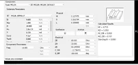
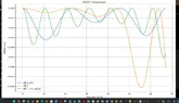
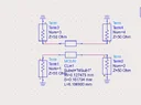
Hello , I tried to build a differential line and controll the SDD21 as shown in the photo.
SDD21=S21-S41

i tried to increase the absolute s41 but the sdd21 is the difference between two complex and as you can see in the photo.
i cant get the sdd21 smaller.
Where did i go wrong?
Thanks.
 
Attachments
  • plot3.webp
    plot3.webp
    38.7 KB · Views: 1
  • plot_calculator.webp
    plot_calculator.webp
    71 KB · Views: 2
  • plot.webp
    plot.webp
    74.7 KB · Views: 1
Engineering news on Phys.org
yefj said:
i cant get the sdd21 smaller.
Where did i go wrong?
Paralysis by analysis.
Perfection is the enemy of progress.

I believe your sdd21 is the S parameter, with differential input, and differential output, of the forward transfer function, from port 1 to port 2.
For what you are doing, any loss below 0.01 dB loss is indistinguishable from perfection. You can model it, but it is unobtainable in the real world.

The impedance mismatch, in the manufacture of the connectors, and in the printing of the real PCB tracks, will exceed that.
 
Hello Baluncore, I was told that there are two kinds of differential lines.
Neck Down and Loosly Coupled.
The difference between them is that Neck down has attenuated SDD21,correct?
I tried to recreate this effect its not working.
How can I design the ND and LC lines to the the difference in SDD21.
Thanks.