manueldois
- 8
- 0
Quantum laser diodes.
How does light escape?
I recently became very interested on the functioning of these amazing devices and so I read online about the topic of quantum wells, semiconductors and lasers.
After much reading I believe I can now understand the basics of lasers, resonant chambers, semiconductors, band-gaps and quantum wells and how they produce light.
Only one point is missing in the puzzle:
After visible light has been created in the thin quantum well layer, how can it escape to the outside world?
How is the light not trapped immediately after it is created, by colliding with the quantum well material? How does it exit the thin quantum well layer? How does light move inside the diode, being it's semiconductor materials opaque? Shouldn't the opaque semiconductor stop and absorb the light like a normal opaque material?
I am aware there are various types of quantum laser diode design but in none I can comprehend: How the light created in the well travels from the quantum well through all the semiconductor material bounding the well to reach outside.
The typical materials used are aluminium gallium arsenide and gallium arsenide for the walls and Indium gallium arsenide for the quantum well.
Are these semiconductors used transparent? Or is a material's transparency not applicable to very small films? Or is there some other mechanism to evacuate light out of the device?
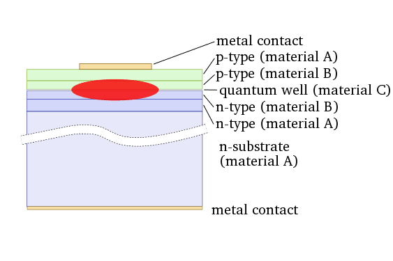
A simple quantum well laser diode:

A Vertical emmiting laser diode:
http://upload.wikimedia.org/wikipedia/en/thumb/4/43/Real_vcsel.svg/720px-Real_vcsel.svg.png
How does light penetrate through all the layers?
There is little information online about quantum lasers, hence why I come to you. If you can provide me with a resource to explain me the inner workings of quantum laser diodes in more detail that'll suffice.
Thank you.
How does light escape?
I recently became very interested on the functioning of these amazing devices and so I read online about the topic of quantum wells, semiconductors and lasers.
After much reading I believe I can now understand the basics of lasers, resonant chambers, semiconductors, band-gaps and quantum wells and how they produce light.
Only one point is missing in the puzzle:
After visible light has been created in the thin quantum well layer, how can it escape to the outside world?
How is the light not trapped immediately after it is created, by colliding with the quantum well material? How does it exit the thin quantum well layer? How does light move inside the diode, being it's semiconductor materials opaque? Shouldn't the opaque semiconductor stop and absorb the light like a normal opaque material?
I am aware there are various types of quantum laser diode design but in none I can comprehend: How the light created in the well travels from the quantum well through all the semiconductor material bounding the well to reach outside.
The typical materials used are aluminium gallium arsenide and gallium arsenide for the walls and Indium gallium arsenide for the quantum well.
Are these semiconductors used transparent? Or is a material's transparency not applicable to very small films? Or is there some other mechanism to evacuate light out of the device?
A simple quantum well laser diode:
A Vertical emmiting laser diode:
http://upload.wikimedia.org/wikipedia/en/thumb/4/43/Real_vcsel.svg/720px-Real_vcsel.svg.png
How does light penetrate through all the layers?
There is little information online about quantum lasers, hence why I come to you. If you can provide me with a resource to explain me the inner workings of quantum laser diodes in more detail that'll suffice.
Thank you.
Last edited by a moderator: