Understanding Quantum Cascade Lasers

Join the discussion
Ask a follow-up here, or get your own question answered by working scientists, mathematicians and engineers — people, not an autocomplete.
Real named experts · corrections over time · the nuance an AI answer skips
3 replies · 2K views
Karl330
Messages
6
Reaction score
1
Hello I am struggling to understand the concept of Quantum cascade lasers. I am doing research on a 20 period In0.33Ga0.67As (3.1 nm)/Al0.90In0.10As (7.2 nm) superlattice and would like to fully understand how a quantum cascade laser works. I also have not taken quantum mechanics yet so I might be a little slow to understand. Here is the question

I keep seeing images like this for a quantum cascade laser. Why does the band energy (y-axis) go down for every layer as shown here and what do the squiggly lines mean (I know these are the electron wavefunctions but I'm not entirely sure I get what is going on)?
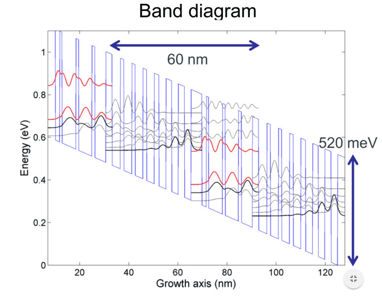
upload_2017-9-5_13-52-52.png


In addition to this how does population inversion happen with each active layer for each electron to get to the highest energy level. Is it some type of pumping from phonons?

Here is what a laser physics book says
The electron leaves the lowest subband by spatial escape to the neighboring conducting region.
 
Physics news on Phys.org
QC lasers are subtle beasts. Let's start with "Why does the band energy (y-axis) go down for every layer as shown here". The answer is that a voltage is applied across an alternating series of high- and low-bandgap materials. The squiggly lines represent electrons tunneling from one well to the next (intraband tunneling), losing energy in discrete amounts as it goes and emitting large numbers of (typically mid-wave IR) photons.

Does that help?
 
I understand that a voltage is applied which sends electrons tunneling through barriers and quantum wells but I am confused on what you mean by high and low bandgap materials. For example a 20 period In0.33Ga0.67As (3.1 nm)/Al0.90In0.10As (7.2 nm) is a superlattice that I am studying and I am confused on how the bandgap changes from layer to layer. I have found this online and also trying to understand it because I thought a quantum well was an area between two thin semiconducting material and here it just says the white InGaAs is a quantum well and the black AlInAs is a barrier.
?temp_hash=515144f176973886e3c339617a486b76.png
 
Karl330 said:
I understand that a voltage is applied which sends electrons tunneling through barriers and quantum wells but I am confused on what you mean by high and low bandgap materials. For example a 20 period In0.33Ga0.67As (3.1 nm)/Al0.90In0.10As (7.2 nm) is a superlattice that I am studying and I am confused on how the bandgap changes from layer to layer. I have found this online and also trying to understand it because I thought a quantum well was an area between two thin semiconducting material and here it just says the white InGaAs is a quantum well and the black AlInAs is a barrier.
View attachment 210434

Your InGaAs material has a bandgap energy of about 0.95 eV (http://www.batop.com/information/Eg_InGaAs.html), and your InAlAs badgap energy is about 1.5 eV. Does that help?