D Latch using Transmission Gates

  • Thread starter Thread starter jaus tail
  • Start date Start date
  • Tags Tags
    Transmission
Join the discussion
Registration is free. Ask a follow-up in this thread, or start your own.
6 replies · 4K views
jaus tail
Messages
613
Reaction score
48
TL;DR
Why is inverter used for D Latch using Transmission Gates?
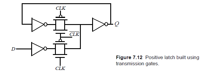
My book has this diagram:
246326

Book: Digital Integrated Circuits by Jan M. Rabaey

I don't understand the purpose of using the three Inverters. It's not mentioned in the book, nor could I find anything on the internet.
 

Attachments

  • 1562670684079.png
    1562670684079.png
    1,018 bytes · Views: 284
Engineering news on Phys.org
Probably because you generally want to buffer all inputs and outputs (to get high input impedance and low output impedance. The only time I've used an unbuffered inverter is in some crystal oscillator circuits...
 
  • Like
Likes   Reactions: jaus tail
jaus tail said:
I don't understand the purpose of using the three Inverters.
Two inversions cancel to make a non-inverting amplifier.

The lower inverter is an input buffer amplifier. Q follows D, through two inverters, while the lower transmission gate is conducting.

The upper two-inverter loop provides a positive feedback digital memory. It holds the last digital output state while the D input is isolated and the upper transmission gate is conducting.

It is a “sample and hold” circuit, applied to a digital signal.
 
  • Like
Likes   Reactions: jaus tail and berkeman
But why do I need inverters? If the two inverters are in series, the output is same as input. I might as well not use them.
 
jaus tail said:
If the two inverters are in series, the output is same as input. I might as well not use them.
With two inverters, if you feed the output of each, back to the input of the other, you have a flip-flop which is a memory element.
 
  • Like
Likes   Reactions: jaus tail
Also maybe it can be that inverter also makes up for voltage drop if any. Like inverter will again either pull up to 5 V or 0 V. Like if memory has output as 5 V, then with time it may degrade to 4.5 V and then to 3 V. If it goes below 2.5 V, it may be treated as logic 0.

So with 2 inverters the 4.5 V is again pulled up, and logic remains high.