jisbon
- 475
- 30
- Homework Statement
- A constant electric field is applied between two ends of a piece of metal. Show that the electric field is given by
##\xi =\dfrac {1}{e}\dfrac {dE}{dx}##
Where E is the electron energy and x is the distance on the sample.
Also, draw the energy band of diagram of the metal with and Without the electric field
- Relevant Equations
- -
So I have just been taught this topic but this question seems to be one of a kind and I can't seem to figure it out.
What I've learnt:
When there is a positive electric field applied to the right, for example, the electrons that are free moving in a crystal (aka conducting band) will oppose the direction and move to the left. On the other hand, the holes in the valence band will move with the direction of the electric field.
However, I was not taught anything about how the above equation works.
Working backwards (I know I'm not supposed to do that but I'm really stuck), I can find that dE/dx is actually the loss/gain of energy of the electron that varies with distance. But why will there be a 1/e infront? I'm not really sure how to even start to prove this equation.
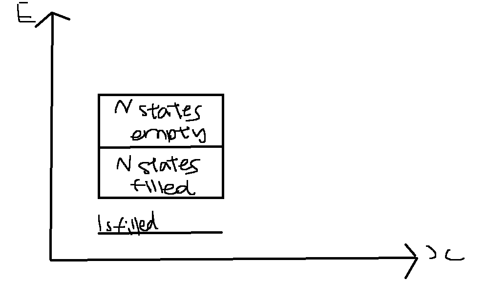
As for part 2, regarding the energy band diagram:

This is what a normal energy band diagram will look like for maybe a 2s band aka Li atom. With the electric field, what would actually change? Since the electrons now create a net displacement, does this mean increased electrical conductivity? If so, how can I represent it on the band diagram? By overlapping or sorts?
Thank you so much.
What I've learnt:
When there is a positive electric field applied to the right, for example, the electrons that are free moving in a crystal (aka conducting band) will oppose the direction and move to the left. On the other hand, the holes in the valence band will move with the direction of the electric field.
However, I was not taught anything about how the above equation works.
Working backwards (I know I'm not supposed to do that but I'm really stuck), I can find that dE/dx is actually the loss/gain of energy of the electron that varies with distance. But why will there be a 1/e infront? I'm not really sure how to even start to prove this equation.
As for part 2, regarding the energy band diagram:
This is what a normal energy band diagram will look like for maybe a 2s band aka Li atom. With the electric field, what would actually change? Since the electrons now create a net displacement, does this mean increased electrical conductivity? If so, how can I represent it on the band diagram? By overlapping or sorts?
Thank you so much.