How is the inversion Channel formed in SOI Mosfet?

Join the discussion
Registration is free. Start your own thread to ask a follow-up.
4 replies · 3K views
jaus tail
Messages
613
Reaction score
48
Hi,
I'm studying MOSFET in detail and I'm struggling to understand how the channel is formed in case of SOI Mosfet.

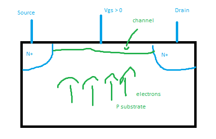
For normal mosfet
upload_2018-10-18_0-37-27.png

A positive Gate to source voltage attracts electrons from P substrate towards Gate and thus a channel is formed.
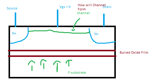
But in case of SOI
upload_2018-10-18_0-40-3.png

There is a buried Oxide film so how will electrons go towards Gate and form the channel? How is the channel formed in SOI Case? I tried google but only came across Fabrication Process of SOI and its advantages and drawbacks.
Any insight would be helpful?
 

Attachments

  • upload_2018-10-18_0-36-58.png
    upload_2018-10-18_0-36-58.png
    2.9 KB · Views: 589
  • upload_2018-10-18_0-37-27.png
    upload_2018-10-18_0-37-27.png
    3.2 KB · Views: 1,346
  • upload_2018-10-18_0-40-3.png
    upload_2018-10-18_0-40-3.png
    3.4 KB · Views: 931
Physics news on Phys.org
The electrons which form the channel flow out of the N+ source and drain.
 
  • Like
Likes   Reactions: jaus tail
Then what is the purpose of dopimdthe substrate with light P doping. I can just use a Normal semiconductor with no doping.
 
You can't really build a semiconductor with no doping. In silicon, for example, to get truly intrinsic silicon (no doping), the impurity level needs to be below the intrinsic free carrier level of about 1E10 atoms/cm^3. Since silicon has about 10^23 atoms/cm^3, this means the material has to be pure to better than the part per trillion level, which is very difficult or impossible. So the substrate will be either lightly N-type or lightly P-type. If it is N-type, then you have an ohmic leakage path between the source and drain. If it is P-type, there are back-to-back diodes between the source and drain, so the leakage is very small.
 
  • Like
Likes   Reactions: jim mcnamara and jaus tail
Thanks. This makes sense that due to fabrication constraints we dope the substrate with light P type. This helps a lot.