Is it possible electrons fallen into holes and go straight to collecto

In summary, an electron that falls into a hole in the base of a transistor will become an electron in the valence band, and will move to the depletion region in the CB junction. There, it will get energy from the VCB exits the valence band and go into the depletion region.
  • #1
anhnha
181
1
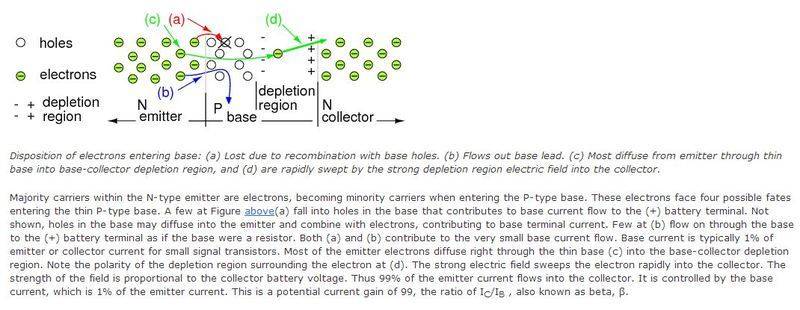
I took this picture from forum aboutcircuits to illustrate current flow in NPN transistor.
attachment.php?attachmentid=59441&stc=1&d=1370918074.jpg

attachment.php?attachmentid=59442&stc=1&d=1370918074.jpg

Here is what I am confused:
A few at Figure above(a) fall into holes in the base that contributes to base current flow to the (+) battery terminal.
Why these electrons that fall into holes necessary flow into base terminal and contribute to base current flow?
Is it possible that there are some electrons fallen into holes and then go straight into collector?

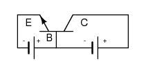
Or in other words:
When an electron in conduction band from emitter falls into hole in base, it become electron in valence band. I wonder where the electron will go.
- the electron now is in valence band and it moves in valence band to positive lead of battery VBE
- the the electron now is in valence band and it moves in valence band to depletion region in CB junction and here it gets energy from VCB exits valence band and go into depletion region.
 

Attachments

  • NPN currents 1.JPG
    NPN currents 1.JPG
    2.6 KB · Views: 489
  • NPN currents.JPG
    NPN currents.JPG
    47.1 KB · Views: 527
Last edited:
Physics news on Phys.org
  • #2
anhnha said:
When an electron in conduction band from emitter falls into hole in base, it become electron in valence band. I wonder where the electron will go.

It's all a matter of context here when we talk of "electrons" and "holes." In this context, when an electron combines with a hole, both vanish.

Of course we know that the electron does not really, physically blink out of existence. But in this context it does. In this context, when we talk about an "electron" we're referring to an "extra" electron -- one that's not in a bound state -- an extra electron that can act as a charge carrier -- an electron that is not presently "inside" a hole.

So in this context, when an electron combines with a hole, the electron disappears. And so does the hole.

[Edit: similarly, in the p-region, the "holes" don't have negatively charged electrons in them, and there are more holes than extra electrons. The holes act as positive charge carriers here in the p-region. And when a hole does combine with an electron, both "vanish" in this context.]
 
  • #3
Hi, I knew that but here is my problem.
We know that P semiconductor can conduct. In this case consider EB junction. When an electron(free electron in emitter) combines with a hole in base, at the same time, there is another electron (valence electron) from base exit valence band and go into base lead, finally go into positive lead of VBE(battery).

I wonder if the similar occcur:
When an electron(free electron in emitter) combines with a hole in base, at the same time, there is another electron (valence electron) from base exit valence band and go into depletion region in CB junction finally go into collector and positive lead of VCB(battery).
 
  • #4
anhnha said:
I wonder if the similar occcur:
When an electron(free electron in emitter) combines with a hole in base, at the same time, there is another electron (valence electron) from base exit valence band and go into depletion region in CB junction finally go into collector and positive lead of VCB(battery).

If I understand you correctly, then yes. :smile: As a matter of fact, that's what happens to most of the electron in the base.

Whenever an electron leaves the valance band in the base, it leaves a hole behind. The holes are left behind, and most of the ("extra") electrons are accelerated to the collector via the depletion region. The holes remain until they recombine with electrons coming from the emitter. That's why there are a lot of holes in the base.

Some of the "extra" electrons exit through the base lead. But most of them diffuse in the valance band, and then exit to the collector (via the depletion region) and leave behind a hole as a result.
 
Last edited:
  • #5
Hello again!
In the image in my original post, they say that when an electron go into base they four possible fates:
a) Lost due to recombination with base holes
My understanding:
After recombination, the electron is in valence band and under the electric field from VBE (battery) it goes to base lead through holes.
My confusion is it possible that the electron after recombination with hole in base, it goes to depletion region in CB juction under electric field from VCB.
( I mean that the electron moves through hole in base and go straight ahead to CB juction under electric field from VCB.)
b) Flows out base lead
My understanding:
Based on the image, I think they mean that the elctron goes to base lead without recombination. In this case, base acts as a resistor.
c) Most diffuse from emitter through thin base into base-collector depletion region
My understanding:
I think they meant that the electron will go straight to CB junction without recombination. And in this case base also acts as a resistor.

My main question is that: Of electrons go to collector is it right that:
- some electrons from emitter to base and collector without recombination. And in this case base acts as a resistor.
-some electrons from emitter then recombination in base, then go though holes and finally go to collector.
I dout about the second, it seems that no books mention the possibility.
Therefore, I am confused. Why the electrons after recombination in base must go to base lead not CB juction?
 
  • #6
I may have worded my response poorly earlier, so I'll try to start over, and answer your questions directly.

anhnha said:
Hello again!
In the image in my original post, they say that when an electron go into base they four possible fates:
a) Lost due to recombination with base holes
My understanding:
After recombination, the electron is in valence band and under the electric field from VBE (battery) it goes to base lead through holes.

When an electron recombines with a hole in in the valance band, that electron becomes bound/attached to a stationary atom in the crystal structure. Neither of them move. Well, that's not totally true. One electron might move to the right if there is a positive atom right next to it. But that can better be thought of as a hole moving to the left.

My confusion is it possible that the electron after recombination with hole in base, it goes to depletion region in CB juction under electric field from VCB.
( I mean that the electron moves through hole in base and go straight ahead to CB juction under electric field from VCB.)

The electron is more likely to stay attached to its atom in the crystal. Occasionally though, thermal vibrations will create a electron-hole pair, such that the electron enters the conduction band (leaving a hole behind), then quickly leaves the depletion region due to the electric field, while the hole is left behind. That's where the excess holes come from. This doesn't happen as often, but it does happen.

b) Flows out base lead
My understanding:
Based on the image, I think they mean that the elctron goes to base lead without recombination. In this case, base acts as a resistor.

That is a fine way to imagine it.

c) Most diffuse from emitter through thin base into base-collector depletion region
My understanding:
I think they meant that the electron will go straight to CB junction without recombination. And in this case base also acts as a resistor.

I believe you are correct. (That was where I may have chosen poor wording in a previous post). Most electrons reach the depletion region without recombining.

My main question is that: Of electrons go to collector is it right that:
- some electrons from emitter to base and collector without recombination. And in this case base acts as a resistor.
-some electrons from emitter then recombination in base, then go though holes and finally go to collector.
I dout about the second, it seems that no books mention the possibility.
Therefore, I am confused. Why the electrons after recombination in base must go to base lead not CB juction?

I believe your first thought is right. Most of the electrons from the emitter exit to the collector without recombination -- the base acts as a resistor.

Some (not most) recombine with holes.

Some (not most) exit though the base lead (again, with the base acting as a resistor).

Some electrons (not most, and this is not even shown in the diagram) originate from thermal vibrations, leaving a hole behind.
 
  • Like
Likes 1 person
  • #7
Thanks, that makes more sense now.
The electron is more likely to stay attached to its atom in the crystal. Occasionally though, thermal vibrations will create a electron-hole pair, such that the electron enters the conduction band (leaving a hole behind), then quickly leaves the depletion region due to the electric field, while the hole is left behind. That's where the excess holes come from. This doesn't happen as often, but it does happen.
Is it possible that the electron will get energy from VCB and breaks covalent bond go into depeltion region?
I think this case is simillar to the move of electrons in the circuit bellow.
Please imagine this circuit including a battery, a resistor and p-semiconductor in series.
In this case, when switch is on, there is a current through the resistor, right?
First, there is an electron from negative pole of battery go into p semiconductor. At the same time, there is another electron in other side of p semiconductor break covalent bond and go into positive pole of battery.
Is that right?
 
  • #8
anhnha said:
Thanks, that makes more sense now.

Is it possible that the electron will get energy from VCB and breaks covalent bond go into depeltion region?
I think this case is simillar to the move of electrons in the circuit bellow.
Please imagine this circuit including a battery, a resistor and p-semiconductor in series.
In this case, when switch is on, there is a current through the resistor, right?
First, there is an electron from negative pole of battery go into p semiconductor. At the same time, there is another electron in other side of p semiconductor break covalent bond and go into positive pole of battery.
Is that right?

In a p type semiconductor, there are acceptor levels very close to the top of the valence band. The electron which brakes covalent bond with its atom, goes onto the acceptor level and makes covalent bond with an acceptor atom or other silicon ion where one electron was missing. That electron is immobile, but it leaves a hole in the valence band, which is filled with an other electron, leaving a hole behind, and so on. The holes move. The holes conduct electricity.

ehild
 
  • #9
Hello,
In a p type semiconductor, there are acceptor levels very close to the top of the valence band. The electron which brakes covalent bond with its atom, goes onto the acceptor level and makes covalent bond with an acceptor atom or other silicon ion where one electron was missing. That electron is immobile, but it leaves a hole in the valence band, which is filled with an other electron, leaving a hole behind, and so on. The holes move. The holes conduct electricity.
I know that but here is my confusion:
In this case (NPN trans) base is also a P-semiconductor, then if there are many electron available in p type, can they move to collector by go though holes?
For example, in this case we don't make base thin instead make it thick and heavy dopping.
Then there will be many electrons recombine into holes. But Why do these electrons (combined) must go to base lead not collector? Both base and collector have positive poles of battery to attract electrons by why they don't go to collector?
I am saying only electrons that recombine in base not free electrons that can go straight to collector.
 
  • #10
anhnha said:
Hello,

I know that but here is my confusion:
In this case (NPN trans) base is also a P-semiconductor, then if there are many electron available in p type, can they move to collector by go though holes?

In a p type semiconductor, the majority charge carriers are the holes. The more the doping concentration the less the number of the free electrons. What do you mean on "many electron available p type"?

anhnha said:
For example, in this case we don't make base thin instead make it thick and heavy doping.
Then there will be many electrons recombine into holes. But Why do these electrons (combined) must go to base lead not collector? Both base and collector have positive poles of battery to attract electrons by why they don't go to collector?
I am saying only electrons that recombine in base not free electrons that can go straight to collector.

I tried to explain in the previous post that the recombined electrons can not move. They are part of the covalent bond. The injected electrons move to the base lead or towards the collector, or those few which get enough energy to escape from the bond and to go into the conduction band. At a given doping concentration, thermal equilibrium means equilibrium amount of free electrons and holes. If some holes recombine with the injected electrons, new holes have to form.

By the way, the base is less doped than the collector, and thin to avoid much recombination and ensure most of the injected electrons to fly through it and sucked by the BC junction into the collector.

ehild
 
  • #11
In a p type semiconductor, the majority charge carriers are the holes. The more the doping concentration the less the number of the free electrons. What do you mean on "many electron available p type"?
I meant that by some way, there are many electrons manage to get to the base.
For example, in this case base is very thick and heavy dopping. Why most electrons go to base not collector?
I don't understand that. To me the base seems uniform everywhere then the holes at surfaces at base and collector are same. Both base and collector leads have positive voltages to attract these electrons. If so why only base get most electrons in this case?
 
  • #12
anhnha said:
I meant that by some way, there are many electrons manage to get to the base.
For example, in this case base is very thick and heavy dopping. Why most electrons go to base not collector?
I don't understand that. To me the base seems uniform everywhere then the holes at surfaces at base and collector are same. Both base and collector leads have positive voltages to attract these electrons. If so why only base get most electrons in this case?

Previously you asked about the recombined electrons. They do not go anywhere.

Otherwise, most of the electrons injected into the base region go over to the collector, and only a small fraction recombine with the holes. In a transistor, the base current is much less than the collector current.

ehild
 
  • #13
Hello,
Sorry I need to go back to some basic concepts.
attachment.php?attachmentid=59473&stc=1&d=1371022388.jpg

In this image, how about current Ic and Ib if base is very thick and heavy dopping?
I see in most books say that Ib is almost equal to Ie and Ic≈ 0 but I can't explain it.
If electrons can go to base lead why it can't go to collector lead as both base and collector leads have positive potentials to attract them?
 

Attachments

  • NPN junction.JPG
    NPN junction.JPG
    10.3 KB · Views: 437
  • #14
If that "base" region is very broad and very heavily dropped, all injected electrons recombine with holes near the EB junction, building up a negative space charge. That repels electrons towards the nearby base lead, and into the positive terminal of the EB battery. The electrons move along the easier way. To reach the collector lead, they need to go through the whole base and the collector region. And all of them have resistance.

Anyway, the base of a normal transition is narrow and less doped as the collector. Your arrangement with a highly doped and broad p region sandwiched between two lightly dropped n type region is not a transistor.

ehild
 
  • #15
Hello,
If that "base" region is very broad and very heavily dropped, all injected electrons recombine with holes near the EB junction, building up a negative space charge. That repels electrons towards the nearby base lead, and into the positive terminal of the EB battery. The electrons move along the easier way. To reach the collector lead, they need to go through the whole base and the collector region. And all of them have resistance.
In this case, is there many electrons injected in base region right at the surface of CB junction?
If so, I think they will be easily swept by electric filed from collector and go to collector as if free electrons.
Most of electrons injected into base will combine with holes. I think the base is uniform and the combination rate of electron and hole at verywhere in base is the same. Then the number of electrons combined with holes at base lead and the base edge right at CB junction are equal.
Why these electrons which combined with holes at base edge right at the surface of CB junction not
go to collector under the electric field?
I assume that VCB is large enough.
 
  • #16
The concentration of electrons combine with holes in base lead and base edge right CB junction are equal, right?
If so why VBE can attract these electrons at base lead while VCB can't attract electrons at base edge right CB junction?
 
  • #17
anhnha said:
Hello,

In this case, is there many electrons injected in base region right at the surface of CB junction?

No. The collector does not inject electrons into the base. The CB junction is reverse biased.


ehild
 
  • #18
I will express my mind more clearly. Hope you can understand what I am saying.
Assuming that there are two electrons injected from emitter to base. Both electrons are combined with holes in base.
After the combination, assume that:
1. The first electron go to base's bottom (near base lead)
2. The second electron go to base surface right before CB junction.
Why the first electron easy go out of the hole and go into the positive pole of VBE while the second electron can't exit the hole and go into collector?
 
  • #19
anhnha said:
I will express my mind more clearly. Hope you can understand what I am saying.
Assuming that there are two electrons injected from emitter to base. Both electrons are combined with holes in base.
After the combination, assume that:
1. The first electron go to base's bottom (near base lead)
2. The second electron go to base surface right before CB junction.
Why the first electron easy go out of the hole and go into the positive pole of VBE while the second electron can't exit the hole and go into collector?
I think there might still be some confusion about what happens when an electron combines with a hole.

When an electron combines with a hole:
  • Physically, the electron doesn't go anywhere. It does not "go out of the hole," "exit the hole," or "go to the surface." It stays put in the location that the hole is. In the case of our diagram, the electron and the hole are removed from the picture. In this case, nothing exits to the base lead nor does anything exit to the collector. Both the electron and hole are frozen in place, and both vanish from the picture. (Electrons might move a little bit, between the valance bands of adjacent atoms as holes move through, but this movement is ignorable.)
  • In the context of the diagram, where all shown "electrons" are really extra electrons (in the conduction band), and all "holes" are lack of electrons in an crystal lattice's valance band, the electron and hole annihilate each other and are erased from the picture, so to speak.

========================

But now let's change the question. Let's ignore electron hole recombination for a moment. Let's also ignore electron/hole generation due to thermal action.

Suppose some electrons come from the emitter and enter the base region (the p-type material). (Here, when I say "electron" I mean an electron in the conduction band. I'm ignoring all bound electrons in the valance band).

Some of them, through diffusion, end up down at the base's lead and ultimately end up at the + terminal of the VBE battery.

But due to the geometry of the BJT (with the base surrounding the emitter, and collector surrounding the base [a 3D cross section might be useful here] -- and in particular the base being very thin between the collector and emitter); and due to the existence of the depletion layer, for every electron leaving the base lead, about a hundred (or so) ultimately end up at the collector (also through diffusion, until accelerated at the depletion region). (All electrons I'm speaking of here originally entered from the emitter.)
 
Last edited:
  • #20
anhnha said:
I will express my mind more clearly. Hope you can understand what I am saying.
Assuming that there are two electrons injected from emitter to base. Both electrons are combined with holes in base.
After the combination, assume that:
1. The first electron go to base's bottom (near base lead)
2. The second electron go to base surface right before CB junction.
Why the first electron easy go out of the hole and go into the positive pole of VBE while the second electron can't exit the hole and go into collector?


The recombined electrons do not move
. They are part of a covalent bond and attached to a pair of atoms. Try to understand that and remember. It was said to you several times.

Electrons do not have personality. Once a conduction electron recombines with a hole it ceases to exist as conduction electron. It just adds extra negative charge to the base.
As the base becomes more negative than in equilibrium, one e charge flows away through the leads into the positive terminals of the batteries, from the existing free electrons in the base (the minority carriers).

During recombination and a free electron leaving the base, the numbers of free electrons and holes in the base change with respect to equilibrium. The balance is restored by an electron breaking a bond and producing a new pair of free electron and free hole.

The electrons traversing the BE junction recombine near it and produce extra charge in that region. If the base is very broad as you said, the depletion region with attracting electric field for the electrons is far away from the BE junction. You have seen that far away from the depleted region, the electric field is zero inside the bulk of the semiconductor. No force drives a free electron towards the CB junction. All phenomena happen near the BE junction, and the extra charge flows away through the base lead.

ehild
 
  • Like
Likes 1 person
  • #21
Hello collinsmark,
I am sorry but it still not clear to me. I will explain my confusion step by step.
Please see the image:
attachment.php?attachmentid=59505&stc=1&d=1371098591.jpg

This is my understanding about how holes move in p type semiconductor.
Is this right?
 

Attachments

  • P type.jpg
    P type.jpg
    12.2 KB · Views: 347
  • #22
Thanks, half of my confusion is solved:smile:
. Once a conduction electron recombines with a hole it ceases to exist as conduction electron. It just adds extra negative charge to the base.
As the base becomes more negative than in equilibrium, one e charge flows away through the leads into the positive terminals of the batteries, from the existing free electrons in the base (the minority carriers).

During recombination and a free electron leaving the base, the numbers of free electrons and holes in the base change with respect to equilibrium. The balance is restored by an electron breaking a bond and producing a new pair of free electron and free hole.
That is really I want to know, but I wonder why the similar don't happen with collector.
I imagine that when collector is connected a battery positive pole then at the base surface right before CB junction there is an electric field and that would cause the similar thing as base do.
You have seen that far away from the depleted region, the electric field is zero inside the bulk of the semiconductor. No force drives a free electron towards the CB junction. All phenomena happen near the BE junction, and the extra charge flows away through the base lead.
haha, my second confusion is here. I think the reason for no electric field is like this:https://www.physicsforums.com/showthread.php?t=695986
But if so how can free electrons can move to collector?
I heard that free elctrons are swept by a strong electric field here.
 
  • #23
anhnha said:
Thanks, half of my confusion is solved:smile:

That is really I want to know, but I wonder why the similar don't happen with collector.
I imagine that when collector is connected a battery positive pole then at the base surface right before CB junction there is an electric field and that would cause the similar thing as base do.

haha, my second confusion is here. I think the reason for no electric field is like this:https://www.physicsforums.com/showthread.php?t=695986
But if so how can free electrons can move to collector?
I heard that free elctrons are swept by a strong electric field here.

There is a strong electric field in the depleted region around the CB junction. If the base is appropriately thin the electrons injected from the base can reach that region before recombining, and sucked away into the emitter.

ehild
 
  • #24
Hello again,
During recombination and a free electron leaving the base, the numbers of free electrons and holes in the base change with respect to equilibrium. The balance is restored by an electron breaking a bond and producing a new pair of free electron and free hole.
I wonder why the similar not happen with collector.
For example there are two electrons enter base and recombine with holes. The numbers of free electrons and holes in the base change with respect to equilibrium. The balance is restored by two electron breaking bonds and producing two new pair of free electron and free hole.
Here I mean that there are two ways to restore balance:
1. an electron breaks a bond and producing a new pair of free electron and free hole at base near base lead.
2. another electron break a bond and producing a new pair of free electron and free hole at the base edge near CB junction
The electrons traversing the BE junction recombine near it and produce extra charge in that region. If the base is very broad as you said, the depletion region with attracting electric field for the electrons is far away from the BE junction. You have seen that far away from the depleted region, the electric field is zero inside the bulk of the semiconductor. No force drives a free electron towards the CB junction.
I think the electric field is zero inside bulk of the semiconductor is always true no matter base think or thick.
Is this right?
 

1. Is it possible for electrons to fall into holes and go straight to the collector?

Yes, this is known as the process of electron-hole recombination and it occurs in semiconductor materials. When an electron falls into a hole, it releases energy in the form of a photon and then can continue to move towards the collector.

2. What is the significance of electron-hole recombination in electronic devices?

Electron-hole recombination is crucial in the functioning of electronic devices such as solar cells and transistors. It allows for the conversion of light or electrical energy into usable electrical energy.

3. Can electrons only fall into holes in semiconductors?

No, electron-hole recombination can also occur in other materials such as insulators and metals. However, it is most commonly observed in semiconductors due to their unique band structure.

4. Are there any factors that affect the rate of electron-hole recombination?

Yes, the rate of electron-hole recombination can be influenced by various factors such as temperature, impurities in the material, and the presence of electric fields. These factors can either increase or decrease the rate of recombination.

5. How does electron-hole recombination contribute to the efficiency of solar cells?

Solar cells rely on electron-hole recombination to convert sunlight into electricity. The recombination process allows for the separation of charge carriers, creating a flow of electrons towards the collector and generating an electrical current. Therefore, the efficiency of solar cells is directly affected by the rate of electron-hole recombination.

Similar threads

Replies
3
Views
704
  • Electrical Engineering
Replies
12
Views
1K
  • Electrical Engineering
Replies
1
Views
721
Replies
1
Views
760
  • Introductory Physics Homework Help
Replies
18
Views
2K
  • Atomic and Condensed Matter
Replies
7
Views
2K
  • Engineering and Comp Sci Homework Help
Replies
2
Views
2K
Replies
5
Views
2K
  • Introductory Physics Homework Help
Replies
3
Views
894
  • Introductory Physics Homework Help
Replies
1
Views
2K
Back
Top