Simulating this cascoded NMOS logic circuit

  • Context: Engineering 
  • Thread starter Thread starter elektro2021
  • Start date Start date
  • Tags Tags
    Circuit Logic
Join the discussion
Ask a follow-up here, or get your own question answered by working scientists, mathematicians and engineers — people, not an autocomplete.
Real named experts · corrections over time · the nuance an AI answer skips
14 replies · 2K views
elektro2021
Messages
6
Reaction score
0
New poster has been reminded to always show their work when starting schoolwork threads
Homework Statement
Size and simulate the circuit (IMAGE BELOW) so that it achieves a 100 ps delay (50-50) using 0.25 μm devices, while driving a 100 fF load on both differential outputs. (VDD = 2.5V) Assume A, B and their complements are available as inputs.
Relevant Equations
vailable common data for nmos are following Vt=0.43(V),Vdsat=0.63(V),k'=115x10^-6 (A/V^2),lambda=0.06(v^-1)
I need help for following exercise from Rabaey - Digital Integrated Circuits: A Design Perspective

Size and simulate the circuit (IMAGE BELOW) so that it achieves a 100 ps delay (50-50) using 0.25 μm devices, while driving a 100 fF load on both differential outputs. (VDD = 2.5V) Assume A, B and their complements are available as inputs.
Available common data for nmos are following Vt=0.43(V),Vdsat=0.63(V),k'=115x10^-6 (A/V^2),lambda=0.06(v^-1)
Please help me.
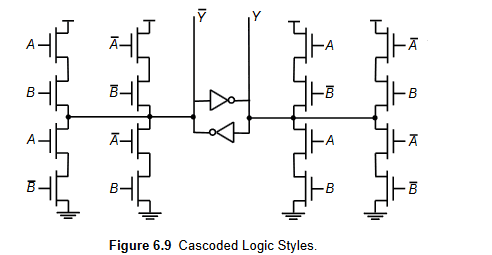
2022-02-04_100733.png
 
on Phys.org
Welcome to PF.
Have you yet identified the two input logic function with a complementary output ?
How will you simulate the gate and delay ?
 
Welcome to PF. :smile:

You need to show some effort before we can provide tutorial help. Please show us how you will approach this question.

Also, I'm a little confused by this symbol in the middle of your NMOS logic circuit -- what is it meant to represent? Is it some IP that is defined elsewhere in the problem statement?

1644244984698.png
 
berkeman said:
Also, I'm a little confused by this symbol in the middle of your NMOS logic circuit
It is a memory element made from two soft output inverters.
It retains the last valid state of the gate, so prevents floating inputs consuming current.
 
  • Informative
Likes   Reactions: berkeman
Baluncore said:
Welcome to PF.
Have you yet identified the two input logic function with a complementary output ?
How will you simulate the gate and delay ?
I think it's a XOR port for Y and XNOR for Y negate.I don't want to simulate the circuit by a simulator but I want to size (by hand) W/L for NMOS transistors to get a 100 ps delay (50-50) using 0.25 μm devices, while driving a 100 fF load on both differential outputs.
 
elektro2021 said:
I don't want to simulate the circuit by a simulator but I want to size (by hand) W/L for NMOS transistors to get a 100 ps delay (50-50) using 0.25 μm devices, while driving a 100 fF load on both differential outputs.
Okay, can you show us how you are going to approach that?
 
I think that I need to compute current charge/discharge for 100 fF capacitor...what do you think?
 
I think that Ic=C*(dv/dt) con C=100 fF and dv/dt= (VDD/2)/T con T=100ps and VDD=2.5V...what do you think?
 
So after you determine the voltages and currents involved, how will you choose the aspect ratio for your geometry?

elektro2021 said:
I want to size (by hand) W/L for NMOS transistors to get a 100 ps delay (50-50) using 0.25 μm devices
 
I don't know...I think that NMOS current depends by W/L...please help me
 
We *are* trying to help. What do your class notes say about aspect ratio effects on voltages and currents?