What is the significance of a -4V gate potential in FET-transistors?

Click For Summary

Discussion Overview

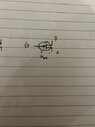
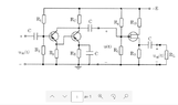
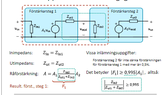
The discussion revolves around the significance of a -4V gate potential in FET-transistors, particularly in the context of circuit design and analysis. Participants explore how this gate potential relates to the operation of P-channel JFETs and its implications for solving circuit problems involving resistances and amplifier stages.

Discussion Character

  • Homework-related
  • Technical explanation
  • Debate/contested

Main Points Raised

  • One participant questions whether the -4V is specified as a pinch-off voltage or an operating voltage, noting that it indicates a P-channel JFET.
  • Another participant clarifies that the potential difference between the gate and source (Vgs) is what matters for operating the FET, and that the gate potential is only equal to Vgs if the source is at ground potential.
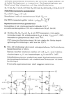
  • A participant expresses uncertainty about the concept of pinch-off voltage and seeks clarification on how to use the -4V gate potential to derive additional equations for solving circuit resistances.
  • Some participants suggest that the gate potential can be used to relate resistances R4 and R5 in a potential divider configuration to achieve the desired gate voltage.
  • Another participant emphasizes the need to solve equations rather than simply selecting resistor values, indicating a structured approach to the assignment.
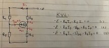
  • One participant proposes using KVL and small-signal analysis to derive equations needed for the circuit design, while expressing uncertainty about how the -4V gate potential contributes to this process.
  • There is a suggestion that the design process may not require solving a complete set of equations, but rather a more intuitive approach to selecting resistor values.

Areas of Agreement / Disagreement

Participants express differing views on whether the gate potential can be used flexibly in design or if a strict equation-based approach is necessary. There is no consensus on the best method to incorporate the -4V gate potential into the circuit analysis.

Contextual Notes

Participants mention specific parameters and conditions related to the circuit design, such as the requirement that the FET-amplifier stage must not lower the first amplifier stage by more than 0.5%. There is also a reference to the complexity of the assignment, with some participants indicating that they have more unknowns than equations.

Who May Find This Useful

This discussion may be useful for students and practitioners interested in FET-transistor operation, circuit design involving JFETs, and those looking for insights into handling complex circuit analysis problems.

David331
Messages
31
Reaction score
1
Homework Statement
The gate potential
Relevant Equations
?
Hi, not really a homework question just a quick question regarding FET-transistor. If the gate potential is -4V does that mean that in the figure below that uGS is -4V. If not, what does it mean and how do you use it in a bigger circuit problem?
 

Attachments

  • 8941E6DC-6973-4F2C-80E5-4EFA2FC173E6.jpeg
    8941E6DC-6973-4F2C-80E5-4EFA2FC173E6.jpeg
    16.5 KB · Views: 174
Physics news on Phys.org
It depends, is the -4V specified as a pinch-off voltage or as an operating voltage?
The symbol is for a P-type channel JFET. They are not common.
The negative voltage is an indication that it has a P-channel, because the gate voltage is measured relative to the more positive source, probably operating with the drain negative.
https://en.wikipedia.org/wiki/JFET#Functions

Search for data and circuits that use a 2N5460, 2SJ174 to 2SJ177, 2SJ270, 2SJ271.
 
For operating a FET the potential difference (voltage) between G and S matters only. Hence, the potential at the gate node is identical to Vgs only in case the source node is at ground potential.
 
Hmm I am kinda new to transistor so I do not know what pinch-voltage is. The full circuit is as below; the source node is not at ground potential. The task of the assignment is to solve for R4, R5, RS, RD with IDQ, UDSQ, UP , IDSS known and that the gate-potential must be -4V ( and that the FET-amplifier stage must not lower the first amplifier stage with more than 0.5%). So then, how could I use that the gate potential is -4V to get an extra equation to solve for the resistances?
 

Attachments

  • 2021-12-07 (11).png
    2021-12-07 (11).png
    10.4 KB · Views: 155
Notice that the negative supply, -E is at the top of the page;
NPN transistors are most common, this circuit uses PNP transistors.
N-chan JFETs are most common, this uses a P-chan JFET.
This is an exercise in thinking upside down.
David331 said:
The gate potential
Relevant Equations:: ?
Hi, not really a homework question just a quick question regarding FET-transistor.
David331 said:
The task of the assignment is to solve for R4, R5, RS, RD with IDQ, UDSQ, UP , IDSS known and that the gate-potential must be -4V ( and that the FET-amplifier stage must not lower the first amplifier stage with more than 0.5%).
You must know more than you are telling us, or you have taken on a difficult first exercise.
David331 said:
The full circuit is as below; the source node is not at ground potential.
The input to the circuit, Uin(t), is referenced to ground. The first two PNP BJTs make a darlington pair, with output referenced to the negative rail. The final JFET stage has input referenced to negative rail, with output voltage referenced to ground.

You need to study common source JFET amplifiers.
They are based on currents flowing through potential dividers.
https://staff-old.najah.edu/sites/default/files/Chapter 9.pdf
 
I can show the entire assignment, although it is in Swedish. I forgot to say, but all the other resistances are known, as well as the h- and g- parameters. I can show you how I am thinking. Firstly I analyze the second amplifier stage using DC and I get the circuit below. I then use KVL to get 3 equations. Now I have 3 equations and 5 unknowns. To get one more equation I will rewrite the ciruit with small-signal analysis and use the demand that the second amplifier stage must now lower the first with more than 0.5%, using picture 3. Lastly, I am thinking that the gatepotential set to -4V should somehow give me a fifth equation so the assignment could be solved, or maybe I am completely wrong...
And yes, I do understand that this is a common source JFET, but how could I use that?
 

Attachments

  • 2021-12-08.png
    2021-12-08.png
    36.9 KB · Views: 197
  • ellära 5.jpg
    ellära 5.jpg
    34.1 KB · Views: 150
  • 2021-12-08 (1).png
    2021-12-08 (1).png
    10.2 KB · Views: 178
Maybe you do not need to solve a set of equations.
You might walk through the design.
R4 and R5 make a potential divider.
Select values that give Vg = -4 V.
Pick Rs to give low output impedance relative to Rload.
 
Hmm I think we are not allowed to pick Rs as you say, even though if it in practice works this way. We "must" solve equations in this way, as the examinator did. But now that you say it, I see that I can relate R4 and R5 with Vg, but how do I do it?
 
It is a potential divider.
i = -E / ( R4 + R5 )
Vg = i * R5
 
  • #10
Oh, of course, thanks for the help. I did not know what potential divider was in Swedish...
 

Similar threads

  • · Replies 5 ·
Replies
5
Views
2K
  • · Replies 2 ·
Replies
2
Views
3K
Replies
8
Views
3K
  • · Replies 6 ·
Replies
6
Views
2K
  • · Replies 3 ·
Replies
3
Views
2K
  • · Replies 4 ·
Replies
4
Views
2K
Replies
9
Views
3K
Replies
22
Views
5K
  • · Replies 3 ·
Replies
3
Views
2K
  • · Replies 1 ·
Replies
1
Views
3K