Designing a Full Bridge SMPS for a 220Vac to 12Vdc Output: A Step-by-Step Guide

In summary, the conversation discusses a question about switching mode power supplies and the difficulty in determining the correct configuration for a full bridge converter with a 220Vac to 12Vdc input and a 12Vdc output. The poster also mentions a second question about optimizing the duty cycle of switches in a converter. Another user responds with potential solutions, including using a cascade design with a boost converter and a buck converter, and providing links for more information on SMPS design.
  • #1
Shahil
117
19
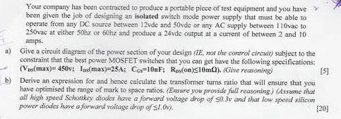
Hey guys ... I have inserted a picture of the question as it was easier to scan than to re-write :P It's based on Switching Mode Power Supplies.
Homework Statement


Q3.jpg

Check the picture or the upload on photobucket http://i91.photobucket.com/albums/k320/shahilj/Q3.jpg" ... It is basically a full bridge config that is required. What got me was that the supply ranges from 220Vac down to 12Vdc BUT the o/p is 12Vdc ... I got a bit confused as to what config to use.

Homework Equations


All equations are to be derived from first principles as such.

The Attempt at a Solution


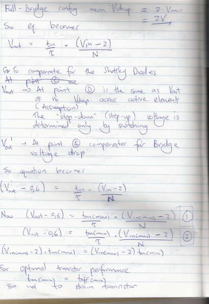
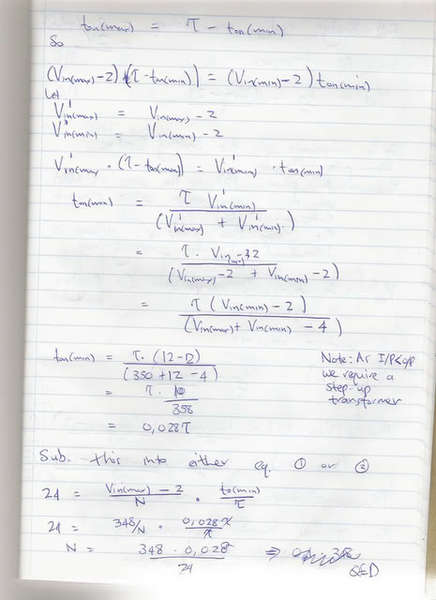
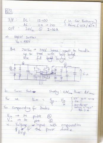
Heres the 3 links first ... http://i91.photobucket.com/albums/k320/shahilj/elec3ans1.jpg"
elec3ans1Small.jpg

elec3ans2.jpg

elec3ans3.jpg


I kinda need someone to at least just check the work .. coz it is worth a lot of marks (25 out of a 100 mark paper) and I really need to know if my method is indeed right!

Thanks so much!
 
Last edited by a moderator:
Physics news on Phys.org
  • #2
Also, had a problem with this question as well :frown:

Honestly, I have no idea where to even start with this one:confused:

Q2.jpg
 
  • #3
hey guys :( seems nobody can help ... um, I've looked on the net for help with the second question I posed ... can't find relevant help anywhere .. please can someone at least guide me in some direction coz I write on Monday and um, well ... I might fail without it!
 
  • #4
Sorry I can't be of too much help in the time required,
but it sounds like the configuration could sanely be
one of several possible ones.

The effect is certainly that of a buck-boost converter
in that you're trying to sometimes boost a smaller
dc voltage up to a higher output voltage.

Yet you're also (over a much wider factor of input
to output voltages) trying to have an efficient buck
converter to step down higher input voltages to lower
output voltages.

It doesn't seem clear that they're saying you should
accomplish the task in any particular circuit configuration,
or with a minimum number of parts.

They're saying to optimize the duty cycle of your switches,
and to give equations that model the thing from first
principles.

Yet also they ignore your control circuit and say you
should only show the power handling circuit.

I'd be tempted to do a cascade design where the boost
stage is activated for only 12vdc to 24vdc input and
it functions as a stand alone boost converter with a
simple topology and a maximum boost of 2:1.

When the DC in is from 24VDC to 707VDC from a
full wave bridge, then you could have a simple buck
converter to reduce that to 24VDC out 2-10A.

Obviously you could get into a bit of trouble with input
voltages within +/- a few volts of 24VDC so that you'd
need to be mindful of your voltage drops in diodes and
resistive losses etc. so that overall it'd still work well in
that region.

Sometimes that's easily done with a 2 stage
approach where a boost converter boosts to a higher
than necessary voltage, then a buck converter takes that
range of higher voltages down to the desired output.

I don't know if that's any easier for you to design and
analyze from first principles or not as opposed to a more
complicated / integrated topology.

Honestly, to me, SMPS circuits are pretty much cookbook
things and you have only so many basic topologies to
choose from and the analyses of those are well known in
many cases.

But since they're apparently not concerned with 'cost'
or control topology or non-ideal effects in the
transformers, capacitors, inductors, you can have a lot
of freedom to design the blocks in ways that are simple
for you to analyze and design even if real world
aspects of size / heat / cost / whatever might cause
some more complicated trade-offs to be made.

You don't even have to show HOW it's controlled, it's
only relevant that SOME pulse train of a reasonable
duty cycle should cause the proper input to output
voltage transformation at the expected range of output
loads, and it's quite arbitrary WHAT that duty cycle is
or HOW you would actually implement the
control / feedback circuit!
 
  • #5
Last edited by a moderator:

1. What is an SMPS?

An SMPS (Switched Mode Power Supply) is an electronic circuit that converts AC power to DC power using switching devices such as transistors and diodes.

2. How does an SMPS work?

An SMPS works by first rectifying the AC input to DC using a rectifier circuit. Then, the DC is chopped into high frequency pulses by a switching device. These pulses are then filtered and regulated to provide a stable DC output.

3. What are the advantages of using an SMPS?

SMPS have several advantages over traditional linear power supplies. They are more efficient, smaller in size, and lighter in weight. They also have a wider input voltage range and can operate at higher frequencies, resulting in less ripple on the output.

4. What are the different types of SMPS?

The most common types of SMPS are flyback, forward, and push-pull. Flyback SMPS are often used in low power applications, while forward and push-pull SMPS are used in higher power applications.

5. How do I design an SMPS?

Designing an SMPS requires knowledge of circuit theory, power electronics, and control systems. It is recommended to consult a textbook or online resources for a step-by-step guide on designing an SMPS. It is also important to follow safety guidelines and use proper components to ensure the reliability and functionality of the SMPS.

Back
Top