ANSYS - Maxwell, current distribution plot?

In summary, current would distribute all around the area, however, one would initially assume that the highest current would be going towards the potential difference applied (which is the lower right bar extending to the right of the page), which I would assume is 1.93 × 10 7 A, and over the furthest left edges possibly low distribution at 1.71 × 10 2 A. However, I'm not sure. Is there a way I could figure this out through ANSYS?
  • #1
PhiowPhi
203
8
I was modeling current distribution in a component:
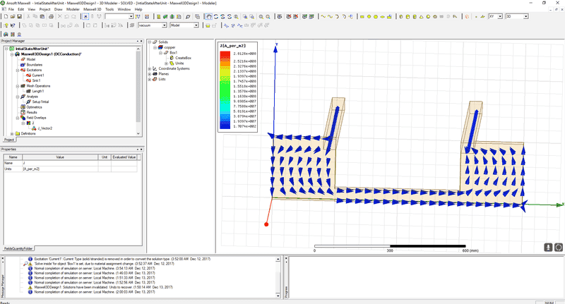
AnalysisHelp1.png


And I plotted the ##\vec J## to simulate & understand the current distribution throughout the conductor, all the flows make sense, however, at the edge of the conductor like so:
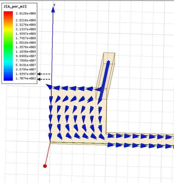
AnalysisHelp2.jpg

Current would distribute all around the area, which is expect. However, one would initially assume that the highest ##\vec J## would be going towards the potential difference applied(which is the lower right bar extending to the right of the page) which I would assume is ##1.93 \times 10^7##, and over the furthest left edges possibly low distribution at ##1.71 \times 10^2##, but I'm not sure. Is there a way I could figure this out through ANSYS?

Even when I apply really higher currents(From 250##A## to 250##kA##) the diagram would change to this distribution:
AnalysisHelp3.jpg


Which leads to the same problem, dark blue being a range of [##1.73 \times 10^2##,##1.93 \times 10^7##] My initial assumption is the least amount of current in that scale list is towards the edges in dark-blue.
 

Attachments

  • AnalysisHelp1.png
    AnalysisHelp1.png
    49.1 KB · Views: 1,763
  • AnalysisHelp2.jpg
    AnalysisHelp2.jpg
    46.5 KB · Views: 1,477
  • AnalysisHelp3.jpg
    AnalysisHelp3.jpg
    50.9 KB · Views: 1,021
Engineering news on Phys.org
  • #2
Please note, that you're plotting a current density. Let's analyze this (from the top left, counter clockwise along the conduction path):
1) Thin conductor (high density, uniform as this is DC).
2) Wide copper plate connected to source and drain on it's corners top and bottom (non uniform current distribution, higher amount of current flows to the right side.. as it's closer to the drain. The more to the left the higher is the resistance as the path length between source and drain gets longer).
3) Thin conductor. Higher current density on the top portion - the same reasons as above.
4) The remaining part is symmetrical to already discussed one.

The problem is in your plot setup - it's the Maxwell's default one. Try to not using it as it may be misleading. Double click on it and set minimal values to zero and maximum as some expected value (adjust it so you'd not reach the peak values on your plot). That way you use all the resolution of the scale plus you will avoid misleading numbers.
 

What is ANSYS Maxwell?

ANSYS Maxwell is a software tool used in computational electromagnetics to simulate and analyze electromagnetic fields and their interactions with materials. It is commonly used in the design and analysis of electrical and electronic systems.

What is a current distribution plot in ANSYS Maxwell?

A current distribution plot in ANSYS Maxwell is a graphical representation of the distribution of electrical current within a three-dimensional model. It shows the magnitude and direction of current flow in different regions of the model, allowing for a better understanding of the behavior of electromagnetic fields.

How is a current distribution plot generated in ANSYS Maxwell?

A current distribution plot is generated in ANSYS Maxwell through a process called finite element analysis. The software discretizes the model into smaller elements and solves for the current flow in each element, which is then combined to create the overall current distribution plot.

What information can be obtained from a current distribution plot in ANSYS Maxwell?

A current distribution plot in ANSYS Maxwell can provide valuable insights into the behavior of electromagnetic fields within a model. It can help identify areas of high current density, locate potential sources of electromagnetic interference, and optimize the design of electrical and electronic systems.

Can a current distribution plot in ANSYS Maxwell be used to validate a design?

Yes, a current distribution plot in ANSYS Maxwell can be used to validate a design by comparing the simulated current distribution with the expected behavior of the system. It can also be used to identify any potential issues or design flaws that may need to be addressed before the system is built.

Similar threads

Replies
10
Views
4K
Replies
10
Views
1K
  • Introductory Physics Homework Help
Replies
1
Views
218
Replies
2
Views
886
  • Introductory Physics Homework Help
2
Replies
44
Views
926
Replies
3
Views
808
  • Electrical Engineering
Replies
8
Views
8K
  • Advanced Physics Homework Help
Replies
4
Views
1K
  • Introductory Physics Homework Help
Replies
25
Views
285
  • Precalculus Mathematics Homework Help
Replies
1
Views
581
Back
Top