Charge Redistribution in a Capacitor Bank/DAC

In summary: C_{ref}## will vary while the circuit is being driven. Clearly, if ##C_{ref}## is huge compared to ##C_1 + C_3## the fluctuation will be minuscule.
  • #1
CoolDude420
198
8
Homework Statement
N/A
Relevant Equations
N/A
I have a question relating DAC architectures. The guts of the question are really to do with capacitors and charge. I want to see if my understanding is correct. This is not a homework question or anything, just thinking about how the circuit interacts.

Setup:

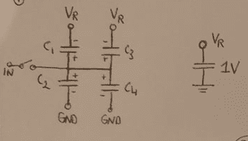
Consider the following setup:
tKi4x.png


Capacitors C1, C2, C3, C4 where C1 = C2 = 32fF and C3 = C4 = 16fF. All the capacitors in the bank have their top/positive plate connected together. The bottom plate of C1 and C3 is connected to a reference capacitor which is charged to 1V initially (Vr node). The bottom plate of C2 and C4 is connected to GND. There is also an input switch used to sample a voltage onto the top plates of each capacitor.

Step 1 - Sampling:
GRdoe.png


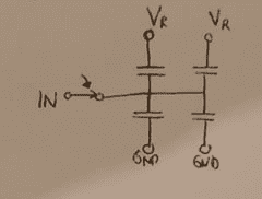
The input switch is closed and the top plates of the capacitors now move with the input voltage (let's say some sinusoid)

Step 2 - Stop Sampling:
6LZ36.png


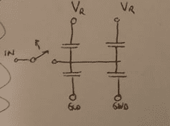
We now open the input switch and a voltage (some voltage of the sinusoid) is sampled on the top plates of each capacitor. Let's call this voltage Vip

Step 3 - Switching:

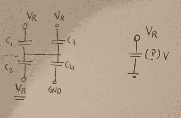
Here come's the tricky part. Let us now switch the bottom plate of capacitor C2 from GND to Vr.
qgSC6.png


Here is my understanding of what happens now:

  1. C2 bottom plate goes from GND to Vr
  2. To ensure that the voltage/hence charge on C2 remains constant, the top plate of C2 must move to Vip + Vr. Just like in a Dickson charge-pump.
  3. Since the top plate of C2 is at Vip + Vr, but the top plates of C1, C3, C4 were still at Vip, charge redistribution occurs.
  4. As part of the charge redistribution process, current (positive charge) flows from the top plate of C2 to the top plates of C1, C3 and C4. The voltage at the common node of all capacitors settles at a steady-state voltage somewhere near Vip + 0.5Vr (I know it can be calculated.)
Here is my question - what happens to the refernece voltage Vr which was on a capacitor?

My guess is that:

  • During the charge redistribution process, positive charge had to leave the top plate of C2 to equalise the potential with other capacitors.
  • Since +Q (positive charge on positive plate) decreased on C2, then -Q (negative charge on negative plate) must also decrease.
  • Thus, electrons flow to the Vr capacitor, thus current leaves Vr capacitor and hence voltage on Vr decreases!
That's one argument. The other argument is that

  • During the charge redistributon process, the positive charge (+Q) gained on the top plates of C1, C3, C4 means that (-Q) charge on bottom plates of C1, C3, and C4 must increase.
  • Thus, electrons flow to the bottom plates of C1, C3, C4 from the reference capacitor, hence current flows to the reference capacitor. Thus, the reference capacitor voltage Vr increases!
These two statements are contradictory. Where is the flaw in my understanding?
 
Physics news on Phys.org
  • #2
Much will depend upon the capacitance value of your reference capacitor. A ginormous capacitance (with respect to the other capacitors) will make changes in voltage cross it insignificant. On the other hand, if it's a similar magnitude of capacitance then there will be some details to consider.

If we combine the two upper capacitors (since they never get rearranged) they become a single 32 fF cap. While the circuit is being driven by the input signal this cap forms a voltage divider with your ##C_{ref}##:

1579901137614.png

The voltage on the lower caps, represented by their sum of 64 fF, is directly driven by ##E##. so it can be ignored here.

You can then see how the voltage on ##C_{ref}## will vary while the circuit is being driven by the input. Clearly, if ##C_{ref}## is huge compared to ##C_1 + C_3## the fluctuation will be minuscule.

If we take an example value of ##C_{ref} = 10 \, \mu F## then the variations on the ##V_{ref}## will have a magnitude of:

##\Delta V_{ref} = E \frac{32 \times 10^{-15}}{32 \times 10^{-15} + 10 \times 10^{-6}} = 3.2 \times 10^{-9} \times |E|##

Assuming that ##|E|## is reasonable you can ignore changes while the circuit is being driven.

After the "switch" of ##C_2##, if ##C_{ref}## is still assumed huge by comparison, it should effectively maintain it's original voltage.
 
Last edited:
  • Like
Likes scottdave
  • #3
gneill said:
Much will depend upon the capacitance value of your reference capacitor. A ginormous capacitance (with respect to the other capacitors) will make changes in voltage cross it insignificant. On the other hand, if it's a similar magnitude of capacitance then there will be some details to consider.

If we combine the two upper capacitors (since they never get rearranged) they become a single 32 fF cap. While the circuit is being driven by the input signal this cap forms a voltage divider with your ##C_{ref}##:

View attachment 256048
The voltage on the lower caps, represented by their sum of 64 fF, is directly driven by ##E##. so it can be ignored here.

You can then see how the voltage on ##C_ref## will vary while the circuit is being driven by the input. Clearly, if ##C_ref## is huge compared to ##C_1 + C_3## the fluctuation will be minuscule.

If we take an example value of ##C_{ref} = 10 \, \mu F## then the variations on the ##V_{ref}## will have a magnitude of:

##\Delta V_{ref} = E \frac{32 \times 10^{-15}}{32 \times 10^{-15} + 10 \times 10^{-6}} = 3.2 \times 10^{-9} \times |E|##

Assuming that ##|E|## is reasonable you can ignore changes while the circuit is being driven.

After the "switch" of ##C_2##, if ##C_{ref}## is still assumed huge by comparison, it should effectively maintain it's original voltage.

My apologies. I forgot to mention one key detail that will change this answer. The reference voltage during the sampling phase is connected to a 1V voltage source to keep it topped up and to charge it back up from any voltage drop in previous conversions. I have updated my explanation below (it didn't let me edit my initial post). I am particularly interested in the drop that occurs on the Cref in step 3 when it doesn't have a 1V source to top it up. You can assume that the Cref capacitor is small.

I'm really just trying to figure out where my charge based explanation is going wrong. Everytime I analyse a capcaitor circuit with +Q and -Q charges moving in my head, I always get confused.

CoolDude420 said:
Homework Statement:: N/A
Homework Equations:: N/A

I have a question relating DAC architectures. The guts of the question are really to do with capacitors and charge. I want to see if my understanding is correct. This is not a homework question or anything, just thinking about how the circuit interacts.

Setup:

Consider the following setup:

View attachment 256012

Capacitors C1, C2, C3, C4 where C1 = C2 = 32fF and C3 = C4 = 16fF. All the capacitors in the bank have their top/positive plate connected together. The bottom plate of C1 and C3 is connected to a reference capacitor which is charged to 1V initially (Vr node). The bottom plate of C2 and C4 is connected to GND. There is also an input switch used to sample a voltage onto the top plates of each capacitor.

Step 1 - Sampling:

1580044314346.png


The input switch is closed and the top plates of the capacitors now move with the input voltage (let's say some sinusoid). Furthermore, during this sampling phase, the reference capacitor is connected to a 1V source to ensure that any reduction in it's voltage from previous conversions is topped up again.

Step 2 - Stop Sampling:


View attachment 256014

We now open the input switch and a voltage (some voltage of the sinusoid) is sampled on the top plates of each capacitor. Let's call this voltage Vip

Step 3 - Switching:

Here come's the tricky part. Let us now switch the bottom plate of capacitor C2 from GND to Vr.

View attachment 256015

Here is my understanding of what happens now:

  1. C2 bottom plate goes from GND to Vr
  2. To ensure that the voltage/hence charge on C2 remains constant, the top plate of C2 must move to Vip + Vr. Just like in a Dickson charge-pump.
  3. Since the top plate of C2 is at Vip + Vr, but the top plates of C1, C3, C4 were still at Vip, charge redistribution occurs.
  4. As part of the charge redistribution process, current (positive charge) flows from the top plate of C2 to the top plates of C1, C3 and C4. The voltage at the common node of all capacitors settles at a steady-state voltage somewhere near Vip + 0.5Vr (I know it can be calculated.)
Here is my question - what happens to the refernece voltage Vr which was on a capacitor?

My guess is that:

  • During the charge redistribution process, positive charge had to leave the top plate of C2 to equalise the potential with other capacitors.
  • Since +Q (positive charge on positive plate) decreased on C2, then -Q (negative charge on negative plate) must also decrease.
  • Thus, electrons flow to the Vr capacitor, thus current leaves Vr capacitor and hence voltage on Vr decreases!
That's one argument. The other argument is that

  • During the charge redistributon process, the positive charge (+Q) gained on the top plates of C1, C3, C4 means that (-Q) charge on bottom plates of C1, C3, and C4 must increase.
  • Thus, electrons flow to the bottom plates of C1, C3, C4 from the reference capacitor, hence current flows to the reference capacitor. Thus, the reference capacitor voltage Vr increases!
These two statements are contradictory. Where is the flaw in my understanding?
 
Last edited:
  • #4
CoolDude420 said:
Here is my question - what happens to the refernece voltage Vr which was on a capacitor?

My guess is that:

  • During the charge redistribution process, positive charge had to leave the top plate of C2 to equalise the potential with other capacitors.
  • Since +Q (positive charge on positive plate) decreased on C2, then -Q (negative charge on negative plate) must also decrease.
  • Thus, electrons flow to the Vr capacitor, thus current leaves Vr capacitor and hence voltage on Vr decreases!
That's one argument. The other argument is that

  • During the charge redistributon process, the positive charge (+Q) gained on the top plates of C1, C3, C4 means that (-Q) charge on bottom plates of C1, C3, and C4 must increase.
  • Thus, electrons flow to the bottom plates of C1, C3, C4 from the reference capacitor, hence current flows to the reference capacitor. Thus, the reference capacitor voltage Vr increases!
These two statements are contradictory. Where is the flaw in my understanding?
In your second scenario you seem to be having electrons coming out of both the top and bottom of the reference capacitor (my assumption is that the "top plates" for C1 though C4 are all connected together at the sampling node). That cannot be true.

Here's a diagram show what I think the circuit will look like in the instant before charge distribution happens. I've combined C1 and C3 into a single capacitor C13. The red arrows represent the voltage orientation on the capacitors (arrow points to positive plates).

1580064988728.png


C13 and C2 are in parallel and of the same size. We can combine them into a single capacitor C123 = 64 fF holding the sum of their charges. That gives us:

1580065601201.png


Where the charges on the capacitors are shown. The red arrows still represent the voltage polarities. Some ##\Delta Q## will leave the reference capacitor. I use conventional current, so this represents the flow of positive charges.

Solve for ##\Delta Q## for a given value of reference capacitor, then you'll be able to see how the voltage on that capacitor changes during charge redistribution.
 
Last edited:
  • #5
gneill said:
In your second scenario you seems to be having electrons coming out of both the top and bottom of the reference capacitor (my assumption is that the "top plates" for C1 though C4 are all connected together at the sampling node). That cannot be true.

Here's a diagram show what I think the circuit will look like in the instant before charge distribution happens. I've combined C1 and C3 into a single capacitor C13. The red arrows represent the voltage orientation on the capacitors (arrow points to positive plates).

View attachment 256142

C13 and C2 are in parallel and of the same size. We can combine them into a single capacitor C123 = 64 fF holding the sum of their charges. That gives us:

View attachment 256144

Where the charges on the capacitors are shown. The red arrows still represent the voltage polarities. Some ##\Delta Q## will leave the reference capacitor. I use conventional current, so this represents the flow of positive charges.

Solve for ##\Delta Q## for a given value of reference capacitor, then you'll be able to see how the voltage on that capacitor changes during charge redistribution.

Thank you for the detailed response. I'm having a hard time following that. In your analysis, Vref is a variable which I understand because charge redistribution will have an effect on it, however Vin is kept constant on the top plates of the capcaitors?
During charge redistrbution, Vin is no longer connected to the top plates, and it should change the voltage on capacitor top plates.

Currently, I'm analysing it in a before and after state. Before charge redistribution, I know all capacitors have Vin on top plates and Vr is constant at 1V, thus I know the charge on every capacitor.
Then I consider the state after charge redistribution has occured. In this state, Vr is an unknown and so is the capacitor top plate voltage. So in this state I have two unknowns.

I then equate the before and after charges (conservation of charge), but I am left with 1 equation with 2 unknowns - capacitor top plate voltage and Vr - the reference voltage.
 
  • #6
CoolDude420 said:
Thank you for the detailed response. I'm having a hard time following that. In your analysis, Vref is a variable which I understand because charge redistribution will have an effect on it, however Vin is kept constant on the top plates of the capcaitors?
During charge redistrbution, Vin is no longer connected to the top plates, and it should change the voltage on capacitor top plates.
What I've presented is the state of the circuit the instant that the "switching" has been made. The input source is no longer connected, and the capacitors are labeled with the potentials and/or charges that they "remember" from the previous instant.
Currently, I'm analysing it in a before and after state. Before charge redistribution, I know all capacitors have Vin on top plates and Vr is constant at 1V, thus I know the charge on every capacitor.
Then I consider the state after charge redistribution has occured. In this state, Vr is an unknown and so is the capacitor top plate voltage. So in this state I have two unknowns.

I then equate the before and after charges (conservation of charge), but I am left with 1 equation with 2 unknowns - capacitor top plate voltage and Vr - the reference voltage.
You'll need to show the work you've done in detail. You may be making things difficult for yourself by choosing a less than optimal strategy, but I can't tell from what you've described so far; I need to see the details of your attempt.
 
  • #7
gneill said:
What I've presented is the state of the circuit the instant that the "switching" has been made. The input source is no longer connected, and the capacitors are labeled with the potentials and/or charges that they "remember" from the previous instant.

You'll need to show the work you've done in detail. You may be making things difficult for yourself by choosing a less than optimal strategy, but I can't tell from what you've described so far; I need to see the details of your attempt.

1580605226695.png

1580605253954.png

1580605259409.png
 
  • #8
Yep. It looks like you're going the long way around. I don't think that you can sum the charges in the way that your doing and hope for conservation of charge. When charge redistribution occurs, some + charges will cancel some - charges.

If you look at the reduced circuit diagram that I provided previously:
1580606736929.png

you should be able to write a KVL equation that reflects how the ##\Delta Q## that leaves the reference capacitor will balance the equation. ##\Delta Q## is going to reduce the potential across ##C_{ref}## and ##C_{123}## while it will increase the potential across ##C_4##. One equation, one unknown (##\Delta Q##).

Once you have ##\Delta Q## you can find the final potentials across all of the capacitors.
 
  • #9
gneill said:
Yep. It looks like you're going the long way around. I don't think that you can sum the charges in the way that your doing and hope for conservation of charge. When charge redistribution occurs, some + charges will cancel some - charges.

If you look at the reduced circuit diagram that I provided previously:
View attachment 256462
you should be able to write a KVL equation that reflects how the ##\Delta Q## that leaves the reference capacitor will balance the equation. ##\Delta Q## is going to reduce the potential across ##C_{ref}## and ##C_{123}## while it will increase the potential across ##C_4##. One equation, one unknown (##\Delta Q##).

Once you have ##\Delta Q## you can find the final potentials across all of the capacitors.
Hmm. I see. However, how do you have only 1 unknown. The Vin voltage on the central node (top plates of capacitors) will also change and so will Vref. Hence, don't you have two unknowns?

Also, I'm a bit confused about this circuit when I think in terms of +Q and -Q charge.
1580611190123.png

For example, if the central (top plate) node increases in voltage, the Q = CV for C123 will increase, thus it now has more charge on it's + plate and hence requires a higher number of - charge on it's bottom plate. The bottom plate of C123 is connected to Cref, so positive charge must flow from C123 bottom plate to top plate of Cref -> thereby increasing the voltage on Cref, not decreasing?
 
  • #10
I have only one unknown because I'm only looking for the net charge that ##C_{ref}## needs to lose in order for the circuit to balance KVL. I have some initial potentials across all the capacitors (hence charge is known on them), and I'm "pushing" some quantity of charge onto each of them, hence changing their individual potential differences. With the right quantity of ##\Delta Q##, KVL will be satisfied.

If you check your initial conditions you'll find that ##V{ref}## is greater than the sum of the potential across ##C_{123}## and ##C_4##. So charge will flow from the top of ##C_{ref}## to the other components. This will have the effect of decreasing the total charge on ##C_{123}## while increasing the charge on ##C_4##.

##C_{123}##'s voltage will decrease while ##C_4##'s will increase. The ##\Delta Q## determines the amount that each decrease or increase. One equation, one unknown (##\Delta Q##).
 
  • #11
gneill said:
I have only one unknown because I'm only looking for the net charge that ##C_{ref}## needs to lose in order for the circuit to balance KVL. I have some initial potentials across all the capacitors (hence charge is known on them), and I'm "pushing" some quantity of charge onto each of them, hence changing their individual potential differences. With the right quantity of ##\Delta Q##, KVL will be satisfied.

If you check your initial conditions you'll find that ##V{ref}## is greater than the sum of the potential across ##C_{123}## and ##C_4##. So charge will flow from the top of ##C_{ref}## to the other components. This will have the effect of decreasing the total charge on ##C_{123}## while increasing the charge on ##C_4##.

##C_{123}##'s voltage will decrease while ##C_4##'s will increase. The ##\Delta Q## determines the amount that each decrease or increase. One equation, one unknown (##\Delta Q##).

Ahh. So essentially you are saying that due to the difference in the initial voltages across the capacitors, the Vref source will supply charge to the other two capacitors.

This charge supplied is what will cause the initial Vref and initial central common node of the two capacitors to change. And so by calculating the amount of charge supplied, we can find new central node voltage and new Vref voltage
 
  • #12
Yes, that's exactly it.
 
  • #13
gneill said:
Yes, that's exactly it.
Thank you!

I just had a thought. Can I still use the law of charge conservation like before but instead do it like this:

1580661741594.png

1580661759042.png


Here is the new part, I relate the new central node voltage with the charge left from the reference capcaitor:
1580663066738.png


And now, I equate the two - charge before and charge after and substitute in this relationship, which gives me one equation and one unknown.

1580661845385.png
 

Attachments

  • 1580661800117.png
    1580661800117.png
    41 KB · Views: 249
Last edited:
  • #14
Well, you can try it and find out if the result matches doing it via KVL. I wrote a KVL equation for the loop:

##\left( V_{ref} - \frac{\Delta Q}{C_{ref}} \right)
+ \left( V_{123} - \frac{\Delta Q}{C_{123}} \right)
- \left( V_{in} + \frac{\Delta Q}{C_{4}} \right) = 0 ##

and solved for ##\Delta Q##.
 
  • #15
gneill said:
Well, you can try it and find out if the result matches doing it via KVL. I wrote a KVL equation for the loop:

##\left( V_{ref} - \frac{\Delta Q}{C_{ref}} \right)
+ \left( V_{123} - \frac{\Delta Q}{C_{123}} \right)
- \left( V_{in} + \frac{\Delta Q}{C_{4}} \right) = 0 ##

and solved for ##\Delta Q##.

Amazing. Thank you very much!
 
  • #16
gneill said:
Yep. It looks like you're going the long way around. I don't think that you can sum the charges in the way that your doing and hope for conservation of charge. When charge redistribution occurs, some + charges will cancel some - charges.

If you look at the reduced circuit diagram that I provided previously:
View attachment 256462
you should be able to write a KVL equation that reflects how the ##\Delta Q## that leaves the reference capacitor will balance the equation. ##\Delta Q## is going to reduce the potential across ##C_{ref}## and ##C_{123}## while it will increase the potential across ##C_4##. One equation, one unknown (##\Delta Q##).

Once you have ##\Delta Q## you can find the final potentials across all of the capacitors.

Why is V123 = 2Vin - Vref? I understand the Vin-Vref voltage is what capacitors C1 and C3 had in the start and after.
I also understand that as soon as you switch (at time t = t0+), that capacitor C2 still has voltage Vin across it, yet it is now in parallel with C1 and C3.

Why are you adding that Vin voltage that C2 had with the voltages across C1 and C3. Seems a bit difficult to understand, since they are all in parallel, so all should same voltage in steady-state.

I understand this isn't steady state, but what's the intuition behind adding them the voltage that C2 had before the switch (Vin) with the voltages that C1 and C3 had before the switch (Vin - Vref)?
 
Last edited:
  • #17
CoolDude420 said:
Why is V123 = 2Vin - Vref?
It isn't. The charge on C123 is given by ##Q_{123} = 32 fF \left(2 V_{in} - V_{ref} \right)##.

Keep in mind that the size of this capacitor is ##C_{123} = 64 fF##...
 
  • #18
gneill said:
It isn't. The charge on C123 is given by ##Q_{123} = 32 fF \left(2 V_{in} - V_{ref} \right)##.

Keep in mind that the size of this capacitor is ##C_{123} = 64 fF##...
Ah, I see. Let me try it by hand now.

Also, side question. Is there any way to use charge redistirbution to do this? I thought that charge redistribution always applies. I tried it with my method that I stated in a previous post, answers look reasonable except they go in a opposite direction. Vref increaes by a small amount rather than decreasing.
 
Last edited:
  • #19
Also, shouldn't C123 = C1 +C2 +C3 = 32fF + 32fF + 16fF = 80fF rather than 64fF?
 
  • #20
CoolDude420 said:
Also, shouldn't C123 = C1 +C2 +C3 = 32fF + 32fF + 16fF = 80fF rather than 64fF?
You're right. For some reason I thought C1 = C3 = 16 fF, and C2 = C4 = 32 Ff.

My method is a form of charge redistribution, only I let Kirchoff do the heavy lifting.
 
  • #21
gneill said:
You're right. For some reason I thought C1 = C3 = 16 fF, and C2 = C4 = 32 Ff.

My method is a form of charge redistribution, only I let Kirchoff do the heavy lifting.

Thanks very much. One last thing, the voltage on Vref should always decrease right? Even in the case where we switch capacitor C1 from Vref to GND (rather than C2 from GND to Vref) and leave everything else the same.
 
  • #22
CoolDude420 said:
Thanks very much. One last thing, the voltage on Vref should always decrease right? Even in the case where we switch capacitor C1 from Vref to GND (rather than C2 from GND to Vref) and leave everything else the same.
Yes, I believe that to be the case. You should be able to run the equations as before to prove it.
 
  • #23
gneill said:
Yes, I believe that to be the case. You should be able to run the equations as before to prove it.
Awesome! Thank you very much!
 

1. What is charge redistribution in a capacitor bank/DAC?

Charge redistribution in a capacitor bank/DAC refers to the process of transferring electric charge from one or more capacitors to another capacitor or set of capacitors. This process is used to control the output voltage or current of the capacitor bank/DAC.

2. How does charge redistribution occur in a capacitor bank/DAC?

In a capacitor bank/DAC, charge redistribution occurs through the use of switches and control circuitry. The switches are used to connect and disconnect capacitors in the bank, allowing for the transfer of charge between them. The control circuitry determines when and how much charge is redistributed.

3. What is the purpose of charge redistribution in a capacitor bank/DAC?

The purpose of charge redistribution in a capacitor bank/DAC is to control the output voltage or current of the bank. By selectively redistributing charge between capacitors, the output can be adjusted to meet specific requirements, such as generating a specific voltage or current.

4. What factors affect charge redistribution in a capacitor bank/DAC?

Several factors can affect charge redistribution in a capacitor bank/DAC, including the capacitance and voltage of the individual capacitors, the switching speed and efficiency of the switches, and the design and performance of the control circuitry.

5. What are the applications of charge redistribution in a capacitor bank/DAC?

Charge redistribution in a capacitor bank/DAC is commonly used in electronic devices and systems that require precise control of output voltage or current, such as power supplies, audio amplifiers, and digital-to-analog converters. It is also used in signal processing and communication systems, as well as in scientific and industrial equipment.

Similar threads

  • Electromagnetism
Replies
16
Views
590
  • Engineering and Comp Sci Homework Help
Replies
13
Views
2K
  • Engineering and Comp Sci Homework Help
Replies
6
Views
1K
  • Introductory Physics Homework Help
Replies
18
Views
1K
  • Engineering and Comp Sci Homework Help
Replies
4
Views
1K
  • Introductory Physics Homework Help
Replies
20
Views
417
  • Engineering and Comp Sci Homework Help
Replies
5
Views
4K
  • Engineering and Comp Sci Homework Help
Replies
8
Views
3K
  • General Math
Replies
1
Views
1K
  • Engineering and Comp Sci Homework Help
Replies
4
Views
2K
Back
Top