DC Blocking Capacitor: Solving a Photodiode Circuit Problem

In summary: So you are just transferring the light pulses through to a PLL that uses it as a frequency input?Yep, that's correct.
  • #1
fonz
151
5
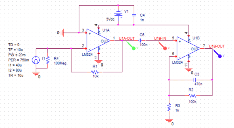
I am modelling a photodiode circuit which produces a small and periodic pulse with a small but potentially variable offset current. My circuit consists of a transimpedance amplifier to convert the small current into a voltage signal. The voltage signal is then filtered by a low pass filter. I wish to remove the small DC offset voltage but I cannot use a subtractor since the DC level may change.

My solution was to place a capacitor at the input of the low pass filter to remove the offset but allow any time-varying signals to be further filtered and amplified by the second stage.

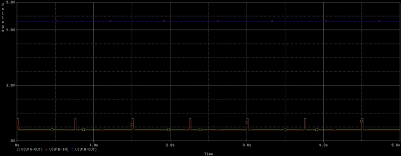
As you can see from my PSPICE simulation, the voltage after the capacitor is only slightly reduced and the DC level is not 0V. The output of my second stage has also satured for some reason.

Some help would be very appreciated!
Schematic.PNG
Capture.PNG
 

Attachments

  • Schematic.PNG
    Schematic.PNG
    24.5 KB · Views: 1,151
  • Capture.PNG
    Capture.PNG
    5.9 KB · Views: 925
Engineering news on Phys.org
  • #2
The + input to U1B needs DC bias. You can't just have a DC open circuit like that at most opamp inputs...
 
  • Like
Likes CWatters
  • #3
Also, you will get a lot better bandwidth performance out of your photodiode if you take its cathode to a negative rail. Can you think of why that is? :smile:
 
  • #4
berkeman said:
Also, you will get a lot better bandwidth performance out of your photodiode if you take its cathode to a negative rail. Can you think of why that is? :smile:

Thanks berkeman, I suspect this is to do with increasing the width of the depletion region in the diode? Unfortunately I don't have a negative rail available in my design.

Regarding your first response, I'm not sure exactly what you mean by this. Through experiment I have discovered that a resistor in parallel with U1B-IN corrects the issue but I don't really want to affect low frequency gain. My circuit needs to operate between 0 and 3 Hz.
 
  • #5
fonz said:
Thanks berkeman, I suspect this is to do with increasing the width of the depletion region in the diode? Unfortunately I don't have a negative rail available in my design.
The width of the region increases, which lowers the capacitance, which increases the bandwidth. But from your 3Hz operating frequency, it sounds like the 0V reverse bias may work.

Nice reference on photodiodes: http://www.osioptoelectronics.com/application-notes/an-photodiode-parameters-characteristics.pdf
fonz said:
Through experiment I have discovered that a resistor in parallel with U1B-IN corrects the issue
Yep :smile:
fonz said:
but I don't really want to affect low frequency gain. My circuit needs to operate between 0 and 3 Hz.
Then you will likely need to do some other kind of circuit for the HPF ("DC blocking" function). I'd look at adding an active filter stage before the output stage maybe. Be sure to look at all of the sources of offsets -- you will get both input Vos and Ios with the LM324 series of opamps.

Maybe just use digital post-filtering to remove the slowly varying offset? Where does the output go? Are you digitizing it?
 
  • Like
Likes fonz
  • #6
Very helpful as always. I'll have a look at alternative op-amps. The output of my second stage goes to a PLL for f-v conversion (this is a purely analogue circuit).

Thanks for the advice.
 
  • #7
fonz said:
The output of my second stage goes to a PLL for f-v conversion (this is a purely analogue circuit).
I think you mean voltage-to-frequency conversion by the PLL, right? Where does the frequency output go?

Wait, or do you mean f-v conversion, with 3Hz being the highest frequency? Yikes that's slow!
 
  • #8
berkeman said:
I think you mean voltage-to-frequency conversion by the PLL, right? Where does the frequency output go?

Wait, or do you mean f-v conversion, with 3Hz being the highest frequency? Yikes that's slow!

In this case f-v conversion and yes 3Hz being the highest frequency. I am yet to test my PLL at such a low frequency (CD4046B). I can't think of an alternative.
 
  • #9
fonz said:
In this case f-v conversion and yes 3Hz being the highest frequency. I am yet to test my PLL at such a low frequency (CD4046B). I can't think of an alternative.
So you are just transferring the light pulses through to a PLL that uses it as a frequency input? Maybe just use a comparator circuit to square things up instead. You could have the comparator threshold adjusting slowly to take out the offset drift, I believe.
 
  • #10
Also, are you required to make this circuit all analog up to the PLL function? This is one of those times when you should consider alternate circuit topologies to optimize the circuit. You could use a microcontroller (uC) for example to digitize the output of the 2nd stage without the DC blocking cap needed, and use digital filtering to condition the signal, and then output the desired analog voltage via a DAC controlled by the uC. There are plenty of inexpensive uCs with internal ADC/DAC combinations...
 
  • #11
Essentially the complete circuit needs to be analogue. To put this into context, I am trying to design an optical heart pulse monitor. I'd be interested to hear more about your comparator suggestion. I'm not sure what you mean by adjusting the comparator threshold slowly?
 
  • #12
fonz said:
I am trying to design an optical heart pulse monitor.
So you have an optical source in an emitter-detector arrangement? What is the light source? I would be modulating the light source at a few kHz at least to help improve the Signal/Noise ratio of the circuit, and it also let's you do your analog filtering and processing at a higher frequency.
fonz said:
I'm not sure what you mean by adjusting the comparator threshold slowly?
You would have a LPF circuit to detect and follow the average value of the circuit (only can vary at 0.1Hz or so), and that will provide the threshold for the comparator circuit. The hysteresis of the comparator circuit needs to be a fair amount smaller than the AC peak value of the pulses, obviously.
 
  • Like
Likes CWatters
  • #13
berkeman said:
So you have an optical source in an emitter-detector arrangement? What is the light source? I would be modulating the light source at a few kHz at least to help improve the Signal/Noise ratio of the circuit, and it also let's you do your analog filtering and processing at a higher frequency.

It's an IR LED. Modulating the source is something i will definitely consider. Thanks for the advice.

berkeman said:
You would have a LPF circuit to detect and follow the average value of the circuit (only can vary at 0.1Hz or so), and that will provide the threshold for the comparator circuit. The hysteresis of the comparator circuit needs to be a fair amount smaller than the AC peak value of the pulses, obviously.

I think I'll give this a go in PSPICE, are you suggesting a cutoff frequency of 0.1Hz?
 
  • #14
fonz said:
I think I'll give this a go in PSPICE, are you suggesting a cutoff frequency of 0.1Hz?
Yeah, something like take the output of the 2nd stage (after you get rid of the DC blocking capacitor), and run that through an active LPF to take the average that can only vary at about 0.1Hz (or slower, depending on your drift), and feed that in as the reference voltage into a comparator circuit. The other input to the comparator circuit is the full AC signal.

Have you designed comparator circuits before? There are a couple of subtleties in how you set the hysteresis voltage.
 
  • Like
Likes fonz
  • #15
berkeman said:
Yeah, something like take the output of the 2nd stage (after you get rid of the DC blocking capacitor), and run that through an active LPF to take the average that can only vary at about 0.1Hz (or slower, depending on your drift), and feed that in as the reference voltage into a comparator circuit. The other input to the comparator circuit is the full AC signal.

Have you designed comparator circuits before? There are a couple of subtleties in how you set the hysteresis voltage.

I've had a go at the averaging filter (see attached). For some reason the DC level is increasing through each stage (even with unity gain). Until I fix this I doubt the comparator will work. Could you take a look and let me know what improvements I can make?

Thanks again
Schematic2.PNG
Capture2.PNG
 

Attachments

  • Schematic2.PNG
    Schematic2.PNG
    24.6 KB · Views: 993
  • Capture2.PNG
    Capture2.PNG
    10.5 KB · Views: 963
  • #16
fonz said:
I've had a go at the averaging filter (see attached). For some reason the DC level is increasing through each stage (even with unity gain). Until I fix this I doubt the comparator will work. Could you take a look and let me know what improvements I can make?

Thanks again
View attachment 219620 View attachment 219621
What is the gain equation for a non-inverting opamp circuit? It's pretty hard to get a gain of 1 through a non-inverting opamp stage, unless it's just a follower with no other functionality... :smile:
 
  • Like
Likes fonz
  • #17
berkeman said:
What is the gain equation for a non-inverting opamp circuit? It's pretty hard to get a gain of 1 through a non-inverting opamp stage, unless it's just a follower with no other functionality... :smile:

Well i won't be making that mistake again. Thanks!

Although now I have a bit of a problem. For the circuit to work I need to go below 0V and I only have a single rail, 5V supply. Without splitting up the rail into +/- 2.5V is there anything else I might be able to do?

Thanks again
Capture3.PNG
Schematic3.PNG
 

Attachments

  • Capture3.PNG
    Capture3.PNG
    15.3 KB · Views: 801
  • Schematic3.PNG
    Schematic3.PNG
    23.8 KB · Views: 768
  • Like
Likes berkeman
  • #18
fonz said:
For the circuit to work I need to go below 0V and I only have a single rail, 5V supply.
Are you talking about needing a negative rail to supply the 3 OP-AMPs?
 
  • #19
fonz said:
lthough now I have a bit of a problem. For the circuit to work I need to go below 0V and I only have a single rail, 5V supply. Without splitting up the rail into +/- 2.5V is there anything else I might be able to do?
Although the LM324 can work with just a single 5V rail, that is really not much headroom to have for most analog processing applications. It's better to run it from at least a 12V rail, and as you have found out, it's nice to have a negative rail for many opamp applications.

If you have enough headroom, you can impose an offset on the input signal, and then process the signal around that offset voltage at each stage. I'll upload a simple circuit that I have used recently to offset a signal that originates near ground, and I needed to do a bit of conditioning before routing it into a single-ended ADC. The power supply for the LM324 opamps in this circuit is only 3.3V, BTW. The top opamp is generating a Vref voltage that the lower circuit is using to offset the ground-referenced input voltage (and reference it to that Vref).

Metro Ckt Snapshot 02 for PF.jpg
 

Attachments

  • Metro Ckt Snapshot 02 for PF.jpg
    Metro Ckt Snapshot 02 for PF.jpg
    17.6 KB · Views: 526
  • Like
Likes fonz
  • #20
NascentOxygen said:
Are you talking about needing a negative rail to supply the 3 OP-AMPs?

Hi Nascent thanks for the comment. The answer is yes because I need the inverting amps to get unity gain which is required for my subtractor to work.

berkeman said:
Although the LM324 can work with just a single 5V rail, that is really not much headroom to have for most analog processing applications. It's better to run it from at least a 12V rail, and as you have found out, it's nice to have a negative rail for many opamp applications.

If you have enough headroom, you can impose an offset on the input signal, and then process the signal around that offset voltage at each stage. I'll upload a simple circuit that I have used recently to offset a signal that originates near ground, and I needed to do a bit of conditioning before routing it into a single-ended ADC. The power supply for the LM324 opamps in this circuit is only 3.3V, BTW. The top opamp is generating a Vref voltage that the lower circuit is using to offset the ground-referenced input voltage (and reference it to that Vref).

Thanks again berkeman. I only have a single 5V rail available for this design so I might need to split up into +3V/-2V for example just to allow the inverting amps to work. It wasn't really what I was aiming for but I can't think of another way of acheiving unity gain and therefore a working subtractor without the inverting stage. Also thanks for the example you have attached I may use a similar circuit to create a virtual ground for my circuit.
 
  • #21
fonz said:
I only have a single 5V rail available for this design so I might need to split up into +3V/-2V for example just to allow the inverting amps to work.
Another option would be to use a simple DC-DC inverter circuit to make a -5V rail for your circuit. You could use a National Instruments Simple Switcher IC and the inductor and diode and capacitor recommended in their Simple Switcher Design Calculator, for example. Also, since you don't need much power from your -5V rail, you could use a simple capacitive inverting charge pump IC to do it. Maybe have a look into those two options to see if they would work for you. :smile:
 
  • Like
Likes CWatters and fonz
  • #22
berkeman said:
Another option would be to use a simple DC-DC inverter circuit to make a -5V rail for your circuit. You could use a National Instruments Simple Switcher IC and the inductor and diode and capacitor recommended in their Simple Switcher Design Calculator, for example. Also, since you don't need much power from your -5V rail, you could use a simple capacitive inverting charge pump IC to do it. Maybe have a look into those two options to see if they would work for you. :smile:

Again, very helpful thanks!
 
  • #23
fonz said:
The answer is yes because I need the inverting amps to get unity gain which is required for my subtractor to work.
I'm sure there are switching regulator chips that will produce a negative supply from a positive, they just need you to provide the inductor.
 
  • #24
fonz said:
Again, very helpful thanks!

NascentOxygen said:
I'm sure there are switching regulator chips that will produce a negative supply from a positive, they just need you just to provide the inductor.
yeah there's lots of them, here's one example that I have used in the past, the ICL7660

https://www.intersil.com/content/dam/Intersil/documents/icl7/icl7660.pdfDave
 
  • Like
Likes berkeman and NascentOxygen
  • #25
fonz said:
I've had a go at the averaging filter
Here's a way to remove the drifting average from vin. It can give some gain, if needed. It might allow you to avoid the need for a negative supply.
circuit.jpg
 

Attachments

  • circuit.jpg
    circuit.jpg
    33 KB · Views: 644
  • Like
Likes Tom.G

What is a DC blocking capacitor?

A DC blocking capacitor is a type of capacitor that is used to block the flow of direct current (DC) while allowing alternating current (AC) to pass through. It acts as a high-pass filter, allowing only high frequency signals to pass through while blocking low frequency signals.

Why is a DC blocking capacitor important in a photodiode circuit?

In a photodiode circuit, the photodiode generates a direct current signal in response to light, which can cause interference or damage to other components in the circuit. The DC blocking capacitor blocks this DC signal, allowing only the desired AC signal to be transmitted through the circuit.

How do I select the right DC blocking capacitor for my photodiode circuit?

The value of the DC blocking capacitor depends on the frequency range of the desired signal and the impedance of the circuit. A larger capacitance value will allow lower frequencies to pass through, while a smaller value will block lower frequencies. It is important to choose a capacitor with a high enough voltage rating to withstand the voltage in the circuit.

What are some common problems that can occur with a DC blocking capacitor in a photodiode circuit?

One common problem is choosing a capacitor with too high of a capacitance, which can result in signal distortion or attenuation. Another problem is using a capacitor with too low of a voltage rating, which can cause the capacitor to fail and potentially damage other components in the circuit.

How do I troubleshoot a problem with a DC blocking capacitor in a photodiode circuit?

If your circuit is not functioning properly, the first step is to check the DC blocking capacitor for any signs of damage or incorrect values. You can also try replacing the capacitor with a different value to see if it improves the circuit's performance. It is also important to make sure all other components in the circuit are functioning correctly.

Similar threads

  • Electrical Engineering
2
Replies
48
Views
2K
  • Electrical Engineering
Replies
15
Views
1K
  • Electrical Engineering
Replies
5
Views
1K
  • Electrical Engineering
Replies
10
Views
2K
  • Electrical Engineering
Replies
13
Views
1K
Replies
26
Views
4K
  • Electrical Engineering
Replies
3
Views
1K
Replies
2
Views
1K
  • Electrical Engineering
Replies
3
Views
1K
  • Electrical Engineering
Replies
10
Views
4K
Back
Top