Explaining a signal converting circuit

In summary, the circuit converts a signal in range [-5,5] V to a range [0,1.2] V. It does this by setting the "analog ground" to 0.6 and attenuating the magnitude of the CV range.
  • #1
gony rosenman
11
4
i have a drawing of a circuit that converts a signal in range [-5,5] V to a range [0,1.2]V .
i wish to understand how it works..
i have basic knowledge of electricity as an undergraduate in general physics but a bit rusty , thus i am here looking for answers...
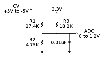
schematic_cv.png
 

Attachments

  • schematic_cv.png
    schematic_cv.png
    2.2 KB · Views: 714
Engineering news on Phys.org
  • #2
It is a "resistive summer" or "passive averager" described in this https://www.allaboutcircuits.com/textbook/semiconductors/chpt-8/averager-summer-circuits/.
 
  • #3
It is indeed a resistive summer. To see that it works (not HOW it works), you can write a nodal analysis equation (using Kirchhoff's current law) at node "ADC" and you will find it gives the function:

ADC = 0.12*CV + 0.6, as desired.

But you want to know HOW it works, here is a more intuitive explanation that is more in the spirit of how an analog engineer would approach the problem (rather than showing you a plug-and-chug simplification of a node equation).

First you need to appreciate that to do the level shifting you really want to do two different things. First, you want to set the "analog ground", or average value, to 0.6 (because that is midway between 0 and 1.2V). Second, you want to attenuate the magnitude of the CV range from 10 V (that is, 5V - (-5V) )to 1.2V. In other words, you want to multiply CV by a gain of 1.2 / 10 = 0.12 and shift its DC level from 0 to 0.6.

OK. Now, to see how the circuit works to do these things we invoke the principle of superposition. This principle states that if we have a linear system then we can calculate the response to each source independently, setting the other sources to zero (in this case CV and the 3.3 V supply) and then add them to get the composite response.

So, we get the baseline by looking at the 3.3 V supply. From the point of view of the 3.3 V supply, we see the 27.4 k and 4.75 k resistors are in parallel (remember we set CV = 0 here). Then, we have a voltage divider and ADC = ((4.75 || 27.4) / ( (4.75 || 27.4) + 18.2)) * 3.3. Now, 4.75 || 27.4 = 4.05 so we have ADC = (4.05 / ( 4.05 + 18.2))* 3.3 = 0.18 *3.3 = 0.6, as desired.

We get the attenuation by looking at what CV "sees". In this case, the 4.75k resistor is in parallel with the 18.2k resistor (remember we set the 3.3 volt source to 0 here). Then we proceed as above, ADC =((4.75 || 18.2) / ( (4.75 || 1.8) + 27.4)) * CV. Or, calculating it out, ADC = 0.12 * CV.

Adding the two responses together (invoking the principle of superposition) we have:

ADC = 0.12*CV + 0.6, which is exactly what we wanted in the first place.

Make sense?
 
  • Like
Likes berkeman, anorlunda, gony rosenman and 1 other person
  • #4
you , my dear sir , are an angel !
thank you for the clear and thorough explanation .
much appreciated :smile::partytime:
 
  • Like
Likes analogdesign, berkeman and anorlunda

Related to Explaining a signal converting circuit

1. How does a signal converting circuit work?

A signal converting circuit is an electronic device that takes an input signal and converts it into a different type of output signal. This can include converting analog signals to digital, or vice versa. The circuit typically consists of different components such as amplifiers, filters, and converters to manipulate and transform the signal.

2. What are the different types of signal converting circuits?

There are various types of signal converting circuits, including analog-to-digital converters (ADC), digital-to-analog converters (DAC), and voltage-to-current converters. Each type is designed to convert a specific type of signal to another form. For example, an ADC converts analog signals to digital, while a DAC converts digital signals to analog.

3. What are the applications of signal converting circuits?

Signal converting circuits are used in a wide range of applications, such as telecommunications, medical devices, audio equipment, and industrial automation. They are also commonly used in electronic devices such as smartphones, laptops, and digital cameras.

4. What factors should be considered when designing a signal converting circuit?

When designing a signal converting circuit, factors such as the input and output signal types, accuracy, speed, and power consumption need to be taken into account. The circuit's components and design must be carefully chosen to ensure the desired conversion is achieved without any loss or distortion of the signal.

5. How can a signal converting circuit be tested and evaluated?

Signal converting circuits can be tested and evaluated using various methods such as simulation software, oscilloscopes, and signal generators. These tools can help analyze the circuit's performance, accuracy, and any potential issues. Additionally, the circuit can be tested in real-world applications to ensure it meets the desired requirements.

Similar threads

  • Electrical Engineering
Replies
13
Views
1K
  • Electrical Engineering
Replies
20
Views
741
Replies
8
Views
1K
Replies
48
Views
4K
  • Electrical Engineering
Replies
12
Views
1K
  • Electrical Engineering
Replies
12
Views
1K
Replies
6
Views
974
  • Electrical Engineering
Replies
5
Views
1K
Replies
2
Views
1K
  • Electrical Engineering
Replies
17
Views
2K
Back
Top