How inversion layer shields electric field?

In summary: Therefore, the gate to body capacitance is zero in linear-mode operation. In summary, in linear-mode operation, the gate to body capacitance (Cgb) is zero because the conducting inversion layer effectively shields the substrate from the gate electric field. This can be mathematically proven using the formula for the capacitance of a parallel-plate capacitor.
  • #1
anhnha
181
1
This question is somewhat relating to electronics but I think it fits better with physics.

The leccture here (slide 13) shows that the gate to body capacitance (Cgb) in linear region is 0. However, there is no explanation at all.

I tried to find the explanation from the reference book and got this:

In linear-mode operation, the inverted channel extends across the MOSFET, between the source and the drain (Fig. 3.31(b)). This conducting inversion layer on the surface effectively shields the substrate from the gate electric field; this Cgb = 0.

With the shielding, does this mean the electric field in substrate is 0?

Is there a way to prove that Cgb = 0 mathematically?

Thank you.
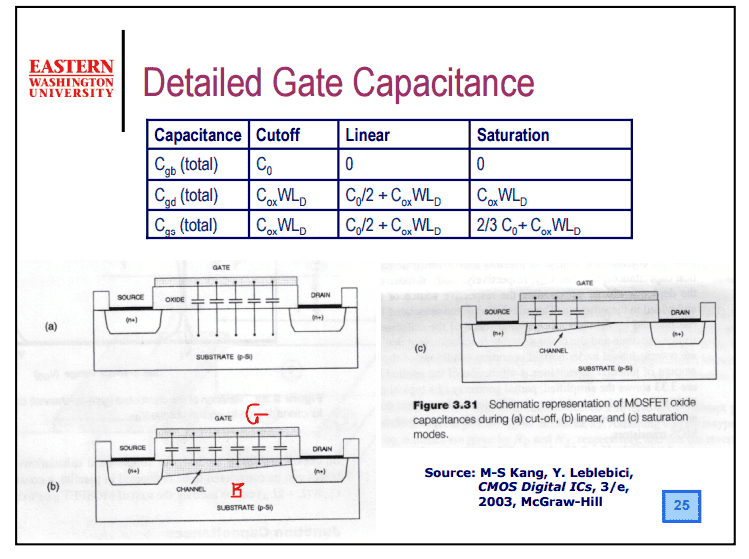
Cgb.PNG
 
Physics news on Phys.org
  • #2
Yes, the electric field in the substrate is zero when the inverted channel extends across the MOSFET. This is because the electric field is generated by the gate voltage and the capacitance between the gate and the body (Cgb). When the channel is extended across the MOSFET, the capacitance between the gate and the body is effectively reduced to zero, since there is no longer an insulating layer between them. To prove that Cgb = 0 mathematically, you can use the formula for the capacitance of a parallel-plate capacitor: C=ε0εrA/dWhere C is the capacitance, ε0 is the permittivity of free space, εr is the relative permittivity, A is the area of the plates, and d is the distance between the plates. When the channel is extended across the MOSFET, d=0, so Cgb=0.
 

1. How does an inversion layer shield electric field?

An inversion layer is a phenomenon that occurs in certain semiconductors when a strong electric field is applied. It causes the majority carriers (electrons or holes) to accumulate near the surface of the material, effectively shielding the electric field from penetrating deeper into the material.

2. What materials exhibit an inversion layer?

Commonly used materials that exhibit an inversion layer include silicon, germanium, and III-V semiconductors such as gallium arsenide (GaAs) and indium phosphide (InP).

3. How does an inversion layer affect device performance?

An inversion layer can have both positive and negative effects on device performance. On one hand, it can improve the breakdown voltage and reduce leakage current in certain devices. On the other hand, it can also cause undesirable effects such as parasitic capacitance and threshold voltage shift in transistors.

4. How can an inversion layer be controlled?

The formation and behavior of an inversion layer can be controlled by varying the doping concentration and type of the semiconductor material, as well as the applied electric field strength. Additionally, the use of surface passivation techniques can also help to mitigate the effects of an inversion layer.

5. Are there any applications of inversion layer shielding?

Inversion layer shielding is commonly used in electronic devices such as field-effect transistors (FETs) and metal-oxide-semiconductor (MOS) capacitors to improve their performance and reliability. It is also a key principle in the operation of photodiodes and solar cells, where it helps to enhance the collection of photo-generated carriers.

Similar threads

  • Introductory Physics Homework Help
Replies
26
Views
596
  • Introductory Physics Homework Help
Replies
6
Views
1K
  • Electromagnetism
Replies
3
Views
2K
  • Introductory Physics Homework Help
Replies
4
Views
3K
Replies
6
Views
2K
  • Electromagnetism
Replies
1
Views
48K
Replies
2
Views
3K
  • Introductory Physics Homework Help
Replies
2
Views
3K
Replies
1
Views
1K
Back
Top