Solving the 1D Poisson equation for a MOS device

In summary, the conversation discussed the development of a 1D Poisson Solver for a MOS device, using a Finite Volume Method and a Newton Solver to solve the equation system numerically. It was noted that there may be a problem with the boundary conditions, which were described as φ(0) = V - Φm + Φs and φ(x_bulk) = 0. The conversation also mentioned the difficulty in accurately measuring doping profiles in smaller processes and the use of curve-fitting models in lieu of first principles. It was recommended to look into the MIT model and historic documentation for a deeper understanding of the derivation of the level 3 model. The importance of considering the gate and channel separately, as well as the voltage at
  • #1
luidgi93
2
0
TL;DR Summary
A question regarding the boundary conditions for the 1D Poisson equation of a MOS devics (Al - SiO2-Si)
Hey everyone,

I'm currently working on a 1D Poisson Solver for a MOS device (Al-Si-SiO2). Therefore, I programmed a Poisson Solver which is appling a boxintegration (Finite Volume Method) through the structure from φ(0) at the metal-oxide interface and φ(x_bulk = 20 nm) in in the silicon bulk. It is solving the equation system numerically with a Newton Solver. The solver is working properly. ρ is calculated through:
ρ = q0 * (Nd - Na - n + p)
with
n = ni * exp(- φ / (kb [eV] * T)) and p = ni * exp( φ/ (kb [eV] * T))

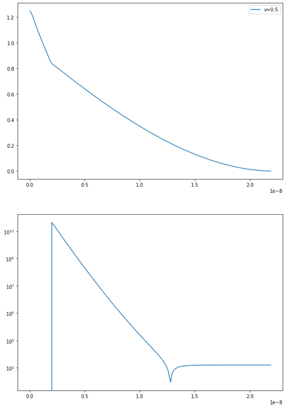
The current solution is for φ (top) and ρ (bottom):
Vg=0.5 example.png

After the oxide-silicon interface at x_ox = 2nm, φ decreases very slowly and doesn't reflect the depletion region. I think that there is a problem with the boundary conditions which are for the moment (with V = 0.5 applied gate voltage in the image):

φ(0) = V - Φm + Φs
with Φm beeing the workfunktion of Al and Φs = χ_si + Eg_si/2 + kb [eV]*T*log(Na/ni)
φ(x_bulk) = 0

I used eps_Si and eps_SiO2 in the box integration for the area of the semiconductor and the oxide. (T = 300 K)

I also tried some variations adding φ_bi (built-in potential) to the boundaries. Could someone please help me and tell me where my mistake is? Is there an interface condition at the SiO2 - Si interface I need to apply?

Thank you very much!
 
Engineering news on Phys.org
  • #2
Why is rho decreasing linearly in the silicon after the Si interface? I suggest you plot out the fixed latice charge(Nd-Na), n, and p all separately so you can see what's going on.
 
  • #3
Thanks for your answer.
I did all that before and it didn’t help me. I can either modify the boundary conditions or the used equations. I checked the calculation of n and p before and they seem reasonable. The values are correct. Na and Nd are fix with Na>Nd. So I really think the problem is in either the equation in the linear system or the boundaries. Could you please answer my question on the boundary conditions?
 
  • #4
So the way you normally derive a MOSFET from "first principles" is embodied in the SPICE level 3 model. Sadly that was one of the last models that was so derived. Since then most modeling is done with curve-fits of "inferior level-3-like models" as a multivariate regression over W and L. This is basically what the Berkeley BSIM family of models do.

The problem behind all of this being that you can not measure doping profiles with any certainty in any process smaller than 10 microns so you can not know the rho value of a Poisson equation. You have to assume with a hand-wave. Otherwise you have somehow assume a profile which can never be proven.

So Level 3 is derived this way:
  1. Write a Gauss' law equation from gate metal to channel surface
  2. Optionally include charge for things like floating gate MOSFETs
  3. Solve/integrate over z for the voltage/potential at the interface between oxide and silicon channel aka the surface potential. You do this for a dx piece of channel.
The reason for needing this voltage is that all of the phenomena of depletion, accumulation and inversion are dependent upon that surface voltage.

This equation then needs to be integration along the channel length though there's an extra piece of information: the charge distribution in that axis. This is an unknown because there's a circular relation between the ensemble of states of the channel, the surface potential and the formation of the state at distance into the channel from the source - one too many unknowns vs. equations so Level 3 punts and allocates charge in thirds.

There are newer models from MIT that may have solved this though it's merely done with yet another empirical variable to indirectly allocate the charge. I'd recommend looking that MIT model as well as historic documentation about the derivation of Level 3.

The key thing: the phenomenology of the gate is different from the channel and that voltage at the surface is key. Not taking that into account is problematic.
 

1. What is the 1D Poisson equation?

The 1D Poisson equation is a mathematical formula used to describe the distribution of electric potential in a one-dimensional system, such as a MOS (metal-oxide-semiconductor) device. It takes into account the charge density and material properties to determine the electric potential at different points in the system.

2. Why is it important to solve the 1D Poisson equation for MOS devices?

MOS devices are commonly used in electronic devices such as transistors, integrated circuits, and memory chips. Solving the 1D Poisson equation allows us to accurately predict the behavior of these devices and optimize their performance. It is also crucial for understanding and improving the reliability of MOS devices.

3. What are the challenges in solving the 1D Poisson equation for MOS devices?

One of the main challenges is accurately modeling the complex behavior of the MOS device, which involves multiple layers and materials. Another challenge is finding an efficient and accurate numerical method to solve the equation, as it involves solving a partial differential equation.

4. How is the 1D Poisson equation solved for MOS devices?

The 1D Poisson equation is typically solved using numerical methods, such as the finite difference method or the finite element method. These methods discretize the equation and solve it iteratively to obtain a numerical solution. Advanced techniques, such as the boundary element method, can also be used for more complex MOS device structures.

5. What are some applications of solving the 1D Poisson equation for MOS devices?

Solving the 1D Poisson equation is essential for the design and optimization of MOS devices in various applications, such as microelectronics, optoelectronics, and sensor technology. It is also used in research and development to study the effects of different device parameters and materials on device performance.

Back
Top