Understanding Valleys in the Conduction Band

In summary, the electrons in a solid will move between the valleys in the conduction band according to Fermi distribution function, but the temperature at which this happens is determined by the effective temperature of the electron and the material's melting point.
  • #1
cr2504life
6
0
Hi and thanks for reading,

I don't really understand the valleys in the conduction band, in the E vs. k diagram, there is the L-valley, r-valley and X-valley. Each has a different momentum... and are at different energy levels.

I understand that at any temperature above absolute zero, a small fraction of electrons will acquire enough energy to jump to the conduction band (overcome the energy gap Eg).

The GaAs bandstructure here:
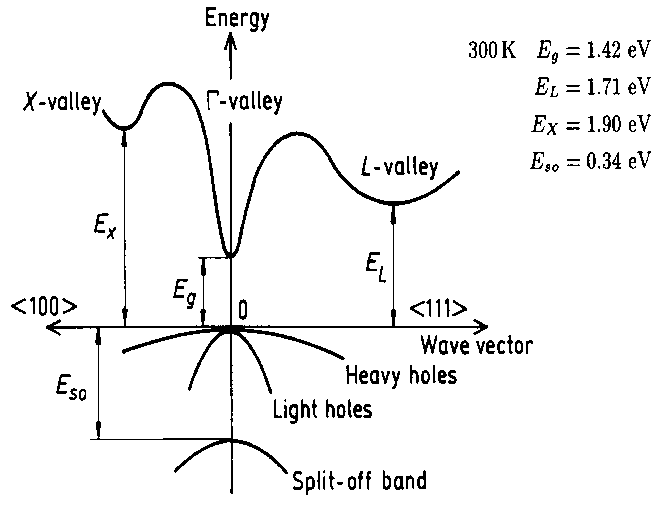
421.gif

http://www.ioffe.ru/SVA/NSM/Semicond/GaAs/bandstr.html

I assume most electrons which acquire enough energy will jump to the lowest valley in the conduction band (r-valley for GaAs).

Ive been trying to determine what is the 'effective' temperature necessary to move an electron from the r-valley to the L-valley, the difference is 0.29 eV in GaAs.
Is the additional thermal energy comming from E = kT ?
... therefore T = 0.29eV*q/(k) ? this is a large temperature ... this seems too large ~3,600 °K.

How do the electons move between valleys ? And how does one find the required energy for this to take place ?
Thanks for any help you can provide.
 
Last edited:
Physics news on Phys.org
  • #2


Although you can tell the required amount of energy an electron needs to jump from valance band top to the conduction band top, you cannot straightforward associate a temperature for this using E=kT. The electrons in a solid are distributed according to Fermi distribution function. And even in the room temperature (kT=0.026meV) a portion of the the Fermi function will reach conduction band. Hence quite handful of electrons will occupy above the conduction band.
http://en.wikipedia.org/wiki/Fermi–Dirac_statistics
 
  • #3


I see from the solution now that the 'effective' temperature of an electron which moves from the r-valley to the L-valley is equal to T = 0.29eV*q/k ~ 3600 K, I had done this correctly.
 
  • #4


cr2504life said:
I see from the solution now that the 'effective' temperature of an electron which moves from the r-valley to the L-valley is equal to T = 0.29eV*q/k ~ 3600 K, I had done this correctly.

Math correct, physics wrong. Think about it, 3600 K, most likely GaAs is a vapour at that temperature, the melting point is 1240 C (1530 K). For an electron to move between the [itex]\Gamma[/itex]-point and L-point of a lattice requires a phonon assist.
 

1. What are valleys in the conduction band?

Valleys in the conduction band refer to regions of low energy in the electronic band structure of a semiconductor or metal. These regions are often described as "valleys" because they are surrounded by higher energy states, similar to how a valley is surrounded by hills.

2. How do valleys form in the conduction band?

Valleys in the conduction band are formed due to the periodic arrangement of atoms in a crystalline material. This arrangement creates energy bands, and the valleys are formed when the energy bands overlap.

3. What is the significance of understanding valleys in the conduction band?

Understanding valleys in the conduction band is important for studying the electronic properties of materials and developing new electronic devices. Valleys can affect the transport of charge carriers and can also play a role in optical and magnetic properties of materials.

4. How are valleys in the conduction band affected by external factors?

External factors such as temperature, electric field, and strain can affect the energy and number of valleys in the conduction band. For example, an applied electric field can change the energy of the valleys and alter their contribution to the overall conductivity of a material.

5. Can valleys in the conduction band be engineered or manipulated?

Yes, valleys in the conduction band can be engineered and manipulated through techniques such as strain engineering, doping, and heterostructure design. These techniques can be used to enhance the performance of electronic devices and create new functionalities.

Similar threads

  • Electrical Engineering
Replies
1
Views
771
  • Atomic and Condensed Matter
Replies
2
Views
4K
  • Atomic and Condensed Matter
Replies
1
Views
6K
  • Atomic and Condensed Matter
Replies
1
Views
1K
  • Atomic and Condensed Matter
Replies
2
Views
3K
  • Engineering and Comp Sci Homework Help
Replies
4
Views
1K
Replies
3
Views
4K
  • Atomic and Condensed Matter
Replies
4
Views
2K
  • Atomic and Condensed Matter
Replies
1
Views
2K
  • Atomic and Condensed Matter
Replies
6
Views
11K
Back
Top