Building a PNP Cascode: A Design Exploration

Click For Summary
SUMMARY

This discussion focuses on the design of a PNP Cascode circuit, contrasting it with the more commonly seen NPN Cascode. Key modifications include converting transistors Q1 and Q2 to PNP types, eliminating the resistor in the emitter of Q2, and adjusting the connections of resistors RC, RE1, RE2, and capacitor CE. Participants emphasize the importance of adhering to the Cascode configuration, which consists of a Common Emitter (CE) stage and a Common Base (CB) stage, while providing specific guidelines for converting NPN circuits to PNP.

PREREQUISITES
  • Understanding of transistor configurations, specifically NPN and PNP types.
  • Familiarity with Cascode amplifier principles, including CE and CB stages.
  • Knowledge of circuit components such as resistors and capacitors.
  • Ability to interpret and modify circuit schematics.
NEXT STEPS
  • Study the design and functionality of Common Emitter (CE) and Common Base (CB) stages in Cascode amplifiers.
  • Learn about the implications of reversing power supply polarity in PNP circuits.
  • Research the role of capacitors in amplifier circuits, particularly the grounding of capacitors like CE.
  • Explore circuit simulation tools to visualize and test PNP Cascode designs.
USEFUL FOR

Electronics engineers, circuit designers, and hobbyists interested in amplifier design, particularly those looking to implement PNP Cascode configurations in their projects.

STEMucator
Homework Helper
Messages
2,076
Reaction score
140
Hi everyone. I have seen the design for an NPN Cascode many times, but I want to build a PNP Cascode. I have scoured the internet for a standard design, but to no avail.

The image below is that of a NPN Cascode. I want to create a PNP cascode by flipping things around. I have placed a red line through the circuitry. On the left side of the red line I expect nothing to change when building the PNP Cascode. On the right side of the red line is where I expect things to change.
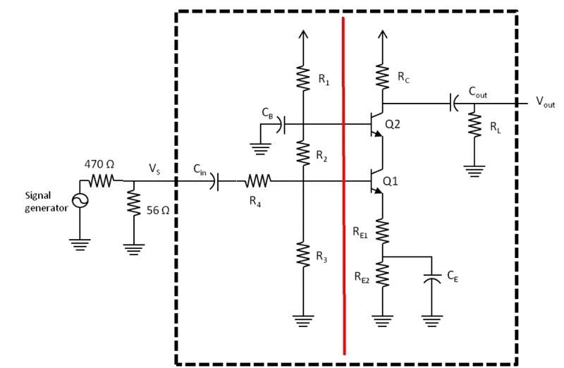
Screen Shot 2015-10-11 at 10.58.45 AM.png


Here is what I am thinking:

1. I will turn transistors ##Q_1## and ##Q_2## into PNP transistors.

2. In the emitter of ##Q_2## there will be no resistor, only the power supply connection ##V_{CC}##.

3. Between the collector of ##Q_2## and the emitter of ##Q_1##, I will place ##R_C## just before the loading circuit. Then I will place the loading circuit.

4. Just after the loading circuit, I will place ##R_{E1}##, ##R_{E2}## and ##C_E##.

5. The collector of ##Q_1## will then be wired to ground.

Does this sound reasonable?

If not, does anyone know what the standard design would look like and could show me?

Thank you.
 
Engineering news on Phys.org
I took the time to make a quick blackboard sketch of what I thought it looks like:

IMG_0963.JPG


Seem reasonable?
 
Your PNP version is wrong, and will not work. The Cascode is CE stage + CB stage.
The correct circuit look like this
 

Attachments

  • M.png
    M.png
    26.3 KB · Views: 817
  • Like
Likes berkeman and STEMucator
Jony130 said:
Your PNP version is wrong, and will not work. The Cascode is CE stage + CB stage.
The correct circuit look like this

It was just hitting me and I came back and saw your post.

I drew this:

https://gyazo.com/d3cfd6526d94f4ce09a6ab1885debf01

It looks pretty much like yours, except the capacitor ##C_E## should be grounded.
 
Zondrina said:
Almost right. R3 resistor must be connected to VCC and R1 to GND.
To convert any NPN circuit into PNP version simply amply this rules:
1 - Change transistor type NPN into PNP
2 - NPN ground now becomes PNP VCC
3 - NPN VCC change to PNP GND (simply reverse the power supply polarity).
4 - If necessary reverse electrolytic capacitor polarity
It looks pretty much like yours, except the capacitor ##C_E## should be grounded.
But this change is not necessary (Vcc is also a good place).
 
Last edited:
Most likely this can only be answered by an "old timer". I am making measurements on an uA709 op amp (metal can). I would like to calculate the frequency rolloff curves (I can measure them). I assume the compensation is via the miller effect. To do the calculations I would need to know the gain of the transistors and the effective resistance seen at the compensation terminals, not including the values I put there. Anyone know those values?

Similar threads

  • · Replies 7 ·
Replies
7
Views
4K
  • · Replies 3 ·
Replies
3
Views
2K
  • · Replies 9 ·
Replies
9
Views
7K
  • · Replies 10 ·
Replies
10
Views
8K
Replies
80
Views
5K
Replies
3
Views
2K
  • · Replies 3 ·
Replies
3
Views
6K
Replies
2
Views
7K
  • · Replies 5 ·
Replies
5
Views
13K
  • · Replies 6 ·
Replies
6
Views
3K