checkmatescott
- 80
- 2
ok without ai quote here goes.
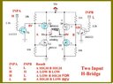
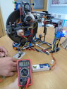
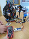
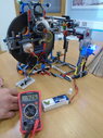
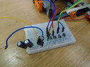
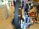
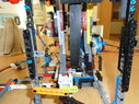
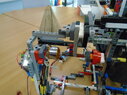
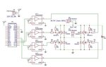
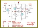
i want to build an h-bridge I have two P-channel IRF9630 and two N-channel IRF630 mosfets laid out in a square. the two N-channel mosfets are at the bottom of the square and the two P-channel mosfets to form the top of the square.
the lower left is the first N-channel mosfet and is labelled Q1, and the top left is the first P-channel mosfet and is labelled Q2, this is the left side. the bottom right is the second N-channel mosfet is labelled Q3 and the top right P-channel mosfet is labelled Q4, this is the right side, there is a 55v vcc.
The gates of the left side are connected via a 10kohm resistor, the gates on the right side are connected via a 10kohm resistor. on the left side, the node which connects to Q2 to the resistor that goes to Q1, the node has a bleed resistor going to source and is called a gate to source bleed resistor and is 10kohm. also on the left side Q1 gate is connected to its source via 10kohm bleed resistor. on the right side, the node which connects to Q4 to the resistor that goes to Q3, the node has a bleed resistor going to source and is called a gate to source bleed resistor and is also 10kohm.
At the node on the left side (where the gate connects to the gate on Q2 through the resistor to Q1, and the bleed resistor that goes to vcc) there is also a bleed resistor 10kohm from Q3 gate to its source. There is a transistor T1 and the collector of that transistor goes to the gate of Q2. the emitter of T1 goes to ground and then the base connects through a 2.2kohm to the digital pin of an arduino (pin 2). At the mirrored node on the right side (which connects to the gates of Q4 to Q3 through the 10kohm resistor and said node is connected to the gate of Q4 goes through the bleed resistor of 10kohm to vcc) there is a transistor T2 and the collector of that transistor goes to the gate of Q4, the emitter of T2 goes to ground and then the base connects through a 2.2kohm to the digital pin of an arduino (pin 3)
Pin 2 and 3 toggle high and low and 50hz to produce an alternating current the drains on the left side are connected and the drains on the right side are connected, between these lines i will be putting a transformer and the current will alternate though the winding exciting the winding at 50hz the sources of the N-channel mosfets will be connected to ground. the sources of the P-channel will be connected to vcc. T1 and T2 are 2n2222 npn transistors.
Okay now i want to know do I have to have a vgs of less than 16 to protect Q2 and Q4 from going over the rated 20 gate to source voltage and I want to do it by voltage divider and zener the zener's I have an assortment of zeners and resistors do you understand P-channel source goes to positive vcc and the N-channel sources goes to ground again the mosfets gates are connected to the collectors of the transistors and the transistors are controlled by arduino.
I hope you can understand and get me a speedy reply i want to know before friday next week? thanks
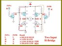
Attachments
Last edited by a moderator: