Doping of semiconductors and fermi energy.

In summary, the addition of a small amount of dopant atoms to a material can significantly change the Fermi energy due to the introduction of a large number of excess charge carriers. This is because the dopant atoms donate or accept a large number of electrons or holes, causing a significant change in the Fermi level.
  • #1
neu
230
3
I understand the principle behind p and n type doping, but I don't understand how such a small amount, 1ppm, can cause such a massive change in the fermi energy.
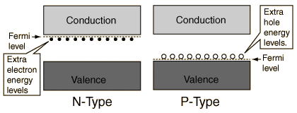
bandop.gif


as I understand it:

for the intrinsic case the number of electrons exactly matches the number of holes and the fermi energy is equal to the mid-gap energy.

When a very small amount of atoms are added which have an extra electron/hole then electrons/holes are added to system which adds extra levels (as in diagram).

But how can such a small addition of electrons/holes have such a large change in the fermi energy?
 
Physics news on Phys.org
  • #2
It's because it introduces a lot of excess charge carriers over that of the intrinsic material. Silicon at 300K has about 10^10 carriers per cc, while 1ppm of dopant donates or accepts about 10^-6 x 10^22 = 10^16 electrons per cc so it significantly changes the Fermi level (chemical potential).
 
  • #3


I can explain this phenomenon by looking at the underlying principles of doping and its effect on the Fermi energy in semiconductors. First, it is important to understand that doping introduces impurity atoms into the crystal lattice of a semiconductor material. These impurity atoms have either one extra electron (for n-type doping) or one missing electron (for p-type doping) compared to the host atoms.

In an intrinsic semiconductor, the Fermi energy is located at the mid-gap energy level because the number of electrons and holes are equal. However, when we introduce impurity atoms, they create additional energy levels in the band structure of the semiconductor. These energy levels are located closer to either the conduction band (for n-type doping) or the valence band (for p-type doping).

Now, when we add a very small amount of impurity atoms, such as 1ppm, these additional energy levels are still present but they are not fully occupied or depleted. This means that there is still a significant number of electrons or holes available at these energy levels. This leads to a change in the Fermi energy, as it shifts towards the energy level with the majority of carriers (electrons or holes).

To put it simply, the small amount of dopant atoms creates a large number of additional energy levels in the band structure, which in turn affects the distribution of electrons and holes and ultimately leads to a change in the Fermi energy. This is why even a small amount of doping can have a significant impact on the Fermi energy in semiconductors.
 

1. What is doping of semiconductors?

Doping of semiconductors is the process of intentionally adding impurities to a semiconductor material in order to alter its electrical properties. This is done to create either p-type (positive) or n-type (negative) semiconductors, which are crucial for the operation of electronic devices.

2. How does doping affect the fermi energy of a semiconductor?

Doping can either increase or decrease the fermi energy of a semiconductor, depending on the type of impurity added. When a p-type impurity is added, the fermi energy decreases, while an n-type impurity causes it to increase. This change in fermi energy allows for the control of electron and hole concentrations in the semiconductor.

3. What is the purpose of controlling the fermi energy in semiconductors?

The fermi energy in semiconductors controls the concentration of free electrons and holes, which are essential for the conduction of electricity. By manipulating the fermi energy through doping, we can control the electrical conductivity, and thus, the functioning of electronic devices.

4. What are the different types of doping methods used in semiconductors?

The two main methods of doping in semiconductors are ion implantation and diffusion. Ion implantation involves firing high-energy ions into the semiconductor material, while diffusion involves heating the material in the presence of a dopant gas. Both methods allow for precise control of the concentration and location of dopants in the semiconductor.

5. Can doping be reversed in semiconductors?

Yes, doping can be reversed through a process called annealing. Annealing involves heating the doped semiconductor material to a high temperature to allow the dopants to diffuse out of the material, restoring its original properties. This is often done during the manufacturing process to create specific regions with different doping concentrations in a semiconductor device.

Similar threads

  • Atomic and Condensed Matter
Replies
3
Views
2K
Replies
1
Views
2K
  • Atomic and Condensed Matter
Replies
3
Views
2K
  • Atomic and Condensed Matter
Replies
5
Views
1K
  • Atomic and Condensed Matter
Replies
1
Views
2K
  • Atomic and Condensed Matter
Replies
3
Views
2K
  • Atomic and Condensed Matter
Replies
2
Views
3K
  • Atomic and Condensed Matter
Replies
0
Views
470
  • Atomic and Condensed Matter
Replies
2
Views
2K
  • Atomic and Condensed Matter
Replies
2
Views
2K
Back
Top