Energy gap between energy bands in solid state physics

In summary, Bragg reflection in solid states at the edge of the first Brillouin Zone results in standing waves at these edges, creating a gap between the energy bands. This can be visualized through the probability density of a symmetric and anti-symmetric standing wave. The energy gap is the difference between the energy of the symmetric and anti-symmetric waves. At the first energy gap, which occurs between band 1 and band 2, Bragg reflection is satisfied at ##k = \pm \pi/a##. This results in a standing wave in the real crystal, where a wave traveling to the right with wavevector ##k = \pi/a## is reflected to travel to the left. This standing wave is generated by the super
  • #1
Gamdschiee
28
2
I know that Bragg reflection in solid states at the edge of e.g. the first Brillouin Zone causes standing waves at these edges, which creates a gap between the energy bands.

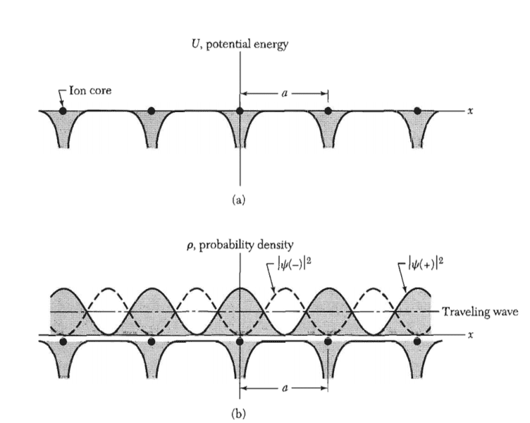
In this picture below you can see the probability density of a symmetric (+) and anti-symmetric (-) standing wave. The energy gap is the difference of the energy of the symmetric wave and the energy of the anti-symmetric wave.
core_potential.png

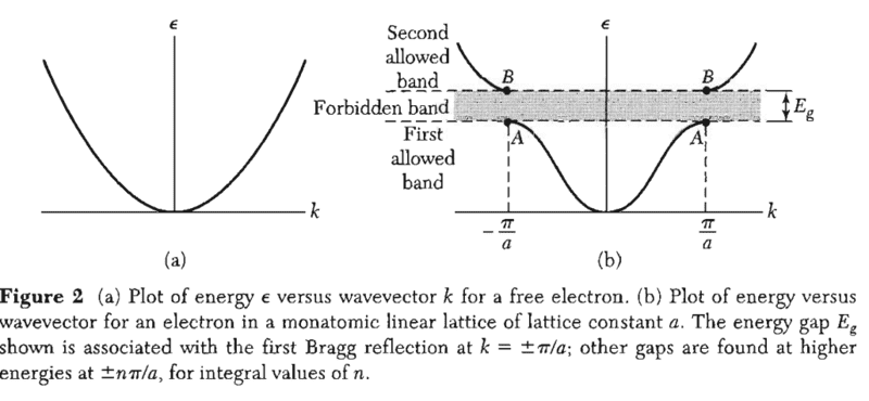
And here you can see the energy gap:
energy_gap.png
It says that the first energy gap(which we see here between band 1 and band 2) occurs due to the bragg reflection at ##k = \pi/a## and ##k = - \pi/a##. The book from Kittel (Solid Sate Physics) also says:
"When the Bragg reflection condition ##k=\pm \pi/a## is satisfied by the wavevector ##\vec k## a wave traveling to the right is Bragg-reflected to travel to the left, and vica versa."

So the wave with the wave vector ##k=\pi/a## (exactly at a bragg plane, which is the edge of a BZ) will be reflected, which creates a standing wave. Or how can you imagine that?
 

Attachments

  • energy_gap.png
    energy_gap.png
    25.2 KB · Views: 1,887
  • core_potential.png
    core_potential.png
    29.4 KB · Views: 1,603
Physics news on Phys.org
  • #2
I agree with you.
In my opinion ## k = {\pi}/{a}## (condition satisfied in the reciprocal space) means that there will be two standing waves (## \psi(+) \text{ and } \psi(-)##) along the direct space, as you can see in your second figure.
 
  • Like
Likes Gamdschiee
  • #3
@Pablo L Martin Thanks for your answer!

But I do not get the origin from such standing wave. Does it come from the waves with wave vector ##\vec k## and ##\vec k - \vec G## ?

Or can you only say in a 1D crystal that a wave traveling to the right with wavevector k = \pi/a (zone edge in reciprocal space) gets reflected in a wave traveling to the left and so there must be a standing wave in the real crystal.

Because in 3D etc the diffracted wave could be go anywere. This is hard to understand. Can anyone help me with this please?
 
Last edited:
  • #4
Gamdschiee said:
@Pablo L Martin

But I do not get the origin from such standing wave. Does it come from the waves with wave vector ##\vec k## and ##\vec k - \vec G## ?

Or can you only say in a 1D crystal that a wave traveling to the right with wavevector k = \pi/a (zone edge in reciprocal space) gets reflected in a wave traveling to the left and so there must be a standing wave in the real crystal.
For this simple 1D case, a wave traveling to the right will reflect to the left if it meets Bragg's condition, which corresponds to ##k=\frac{\pi}{a}##. Since Bragg scattering is an elastic process and we are constrained to 1D, the scattered wave will bounce directly backward with ##k' = -\frac{\pi}{a}##. This can also be worked out mathematically by applying your above stated Bragg equation ##\mathbf k' = \mathbf k + \mathbf G##. It is the superposition of the same electron's initial and scattered wave function that sets up the standing waves. You can generate the standing waves from the initial and final plane wave function ##\exp(\pm i\pi x/a)##. This is how you get the standing waves of form:
##\psi(+) = \exp(i\pi x/a) + \exp(-i\pi x/a) = 2\cos(\pi x/a)##
##\psi(-) = \exp(i\pi x/a) - \exp(-i\pi x/a) = 2i\sin(\pi x/a)##
If you want to visualize this more clearly in your mind in terms of classical standing waves, then the Brillouin zone boundary ##k = \frac{\pi}{a}## corresponds to a wave traveling down a string with wavelength ##\lambda = \frac{2\pi}{k} = 2a## where the lattice spacing ##a## is now just the distance between the endpoints of the string. ##\psi(+)## corresponds to both endpoints free (which sets up a node centered between the endpoints) while ##\psi(-)## corresponds to both endpoints fixed (which sets up nodes at the endpoints). Note that one end fixed and one end free is not allowed because this requires meeting the condition that ##a = \frac{n\lambda}{4}## where n is an odd integer. However, since Bragg's condition requires ##\lambda = \frac{2a}{m}## where m is any positive integer, then combining these conditions gives ##n = \frac{2}{m}##. Hence, no odd integer n exists.

Gamdschiee said:
@Pablo L Martin
Because in 3D etc the diffracted wave could be go anywere. This is hard to understand. Can anyone help me with this please?
In higher dimensions nothing much has changed. As an elementary example consider an electron with ##\mathbf k = k_{x} \hat {\mathbf x} + k_{y} \hat {\mathbf y}## that hits a reciprocal lattice vector ##\mathbf G = -\frac{2\pi}{a} \hat {\mathbf x}##. Thus, we have that ##\mathbf k' = \mathbf k + \mathbf G = (k_{x}-\frac{2\pi}{a} ) \hat {\mathbf x} +k_{y}\hat {\mathbf y}##. From the Bragg condition ##k^{2} = |\mathbf k + \mathbf G|^{2}## we get that ##k_{x} = \frac{\pi}{a} ## an so taken together
##\mathbf k = \frac{\pi}{a} \hat {\mathbf x} + k_{y} \hat {\mathbf y}##
##\mathbf k' = -\frac{\pi}{a} \hat {\mathbf x} + k_{y} \hat {\mathbf y}##
Note that the since ##\mathbf G## is along the x-direction, the Bragg condition required ##k_{x}## to be a specific value. However, ##k_{y}## is allowed to remain arbitrary. Thus, the diffracted beam in higher dimensions is not free to go anywhere, there is a direct bounce back (like in 1D) for the momentum projection along ##\mathbf G##. The upshot of this is that now when we put together the superposition of our initial and final plane waves we get that
##\psi(+) =\exp(ik_{y}y) \left( \exp(i\pi x/a) + \exp(-i\pi x/a)\right) = 2\exp(ik_{y}y)\cos(\pi x/a)##
##\psi(-) = \exp(ik_{y}y) \left( \exp(i\pi x/a) - \exp(-i\pi x/a)\right) = 2i\exp(ik_{y}y)\sin(\pi x/a)##
So we see that an arbitrary phase is added into the standing wave solution. However, the electron density is given by the modulus and so this arbitrary phase disappears.
 
  • Like
Likes Rzbs and Gamdschiee
  • #5
@SpinFlop I see, thank you for the accurate answer. That made me to understand it way more than before. But I still have a few questions below.

1. I know that the energy gap is just the energy difference from the energies of both standing waves ##\psi(+)## and ##\psi(-)## at that exact zone edge:
band_gap.png

Which shows this picture very good. The black band corresponds to a free electron. The red one to ##\psi(+)## and the blue one to ##\psi(-)##.

Also due to the periodicity the energy band of purely free electron looks like:
free_electron.png


So when we have a 'nearly' free electron there will simply be a energy gap as it shows in the first picture above. The created standing waves merge electrons either on the lattice atoms(##-##) location or inbetween (##+##) them.

But in the end I do not understand yet how the first band (red one) and the second band (blue one) are determined. Like e.g. why is there exactly a standing wave ##\psi(+)## and ##\psi(-)##? So why two standing waves at the same time, which creates the gap and so the first band and second band shown in the first picture I uploaded.

For me is it logically when I send a wave to wall and it gets reflected back there will be a simple standing wave. But why two? How are the two parabola at ##k=0## and ##k=2\pi/a## connected to this topic/each other?
 

Attachments

  • band_gap.png
    band_gap.png
    10.2 KB · Views: 1,367
  • free_electron.png
    free_electron.png
    3.4 KB · Views: 1,033
Last edited:

FAQ: Energy gap between energy bands in solid state physics

What is the energy gap in solid state physics?

The energy gap in solid state physics refers to the difference in energy levels between the valence band (highest occupied energy band) and the conduction band (lowest unoccupied energy band) in a solid material. This energy gap plays a crucial role in determining the electrical and optical properties of the material.

What causes the energy gap in solid state materials?

The energy gap in solid state materials is caused by the arrangement of atoms and electrons in the material. In a crystalline solid, the atoms are arranged in a regular and repeating pattern, creating a periodic potential for the electrons. This potential creates energy bands, with the valence band being completely filled and the conduction band being empty, separated by an energy gap.

How does the energy gap affect the electrical conductivity of a material?

The energy gap significantly affects the electrical conductivity of a material. Materials with a smaller energy gap have more electrons in the conduction band, making it easier for them to move and conduct electricity. Conversely, materials with a larger energy gap have fewer electrons in the conduction band, making it more difficult for them to conduct electricity. This is why semiconductors, which have a moderate energy gap, are commonly used in electronic devices.

Can the energy gap be manipulated in solid state materials?

Yes, the energy gap can be manipulated in solid state materials through various methods such as doping (introducing impurities) or applying external forces like pressure. These techniques can alter the energy band structure and thus change the size of the energy gap. This manipulation is vital in creating materials with specific properties for different applications.

What is the relationship between the energy gap and the color of a material?

The energy gap plays a crucial role in determining the color of a material. When light is incident on a material, its energy can be absorbed by the electrons in the material, causing them to jump from the valence band to the conduction band. The energy gap determines the minimum amount of energy required for this jump, and the color of the material is determined by the energy of the absorbed light. For example, a material with a smaller energy gap will absorb higher energy (shorter wavelength) light, appearing blue or violet, while a material with a larger energy gap will absorb lower energy (longer wavelength) light, appearing red or yellow.

Similar threads

Replies
7
Views
2K
Replies
10
Views
2K
Replies
2
Views
4K
Replies
6
Views
2K
Replies
3
Views
2K
Replies
15
Views
7K
Replies
2
Views
1K
Back
Top