Investigating Unexpected Voltage in PSPICE Simulation

Click For Summary
SUMMARY

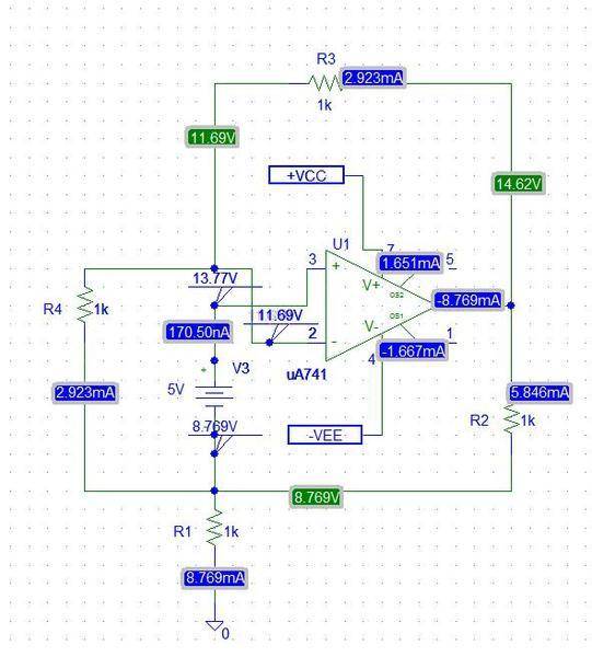
The discussion centers on unexpected voltage readings in a PSpice simulation involving an operational amplifier (op-amp) circuit using the uA741 model. The non-inverting terminal voltage is observed at 13.77V despite a 5V DC source being connected, due to the source being connected between an 8.769V point and the non-inverting input. The circuit's saturation is explained by the op-amp's gain of 200 V/mV, leading to discrepancies in expected voltages. To achieve ideal op-amp behavior in simulations, users are advised to select the "OPAMP" from the "ANALOG" library and adjust voltage limits accordingly.

PREREQUISITES
  • Understanding of operational amplifier principles and configurations
  • Familiarity with PSpice simulation software, specifically versions 9.1 and 9.2
  • Knowledge of circuit analysis techniques, including nodal analysis
  • Experience with the uA741 op-amp model and its characteristics
NEXT STEPS
  • Learn how to configure ideal op-amps in PSpice simulations
  • Research the characteristics and limitations of the uA741 op-amp model
  • Explore advanced circuit analysis techniques to complement simulation results
  • Investigate the impact of voltage supply limits on op-amp performance in simulations
USEFUL FOR

Electrical engineers, circuit designers, and students working with operational amplifiers and PSpice simulations who seek to understand voltage discrepancies in their circuit designs.
reddvoid
Messages
118
Reaction score
1
This is the snap shot i took from Pspice simulation
attachment.php?attachmentid=47753&stc=1&d=1338302911.jpg

I have a doubt here
***why is voltage at non inverting terminal is 13.77V even though i connected 5V dc source to it and why the voltages at inverting and non inverting terminals are not almost same ( which we consider while solving opamp circuits)

thank you .
 

Attachments

  • untitled.JPG
    untitled.JPG
    36.6 KB · Views: 673
Engineering news on Phys.org
Normally, when someone says they connected a 5v source to a point they mean they connected a voltage source between that point and ground. But in the schematic, it shows the 5v source connected between that (strange) 8.769V point and the non-inverting input. So naturally it is going to make the non-inverting input 8.769 + 5.00 = 13.769V.

Is this a schematic you thought up? What is it supposed to do or show?
 
I have exactly resimulated your circuit.

attachment.php?attachmentid=47755&stc=1&d=1338305322.png


I've also opened "eval.lib" and found the macromodel

Code:
*-----------------------------------------------------------------------------
* connections:   non-inverting input
*                |  inverting input
*                |  |  positive power supply
*                |  |  |  negative power supply
*                |  |  |  |  output
*                |  |  |  |  |
.subckt uA741    1 2 3 4 5
*
  c1   11 12 8.661E-12
  c2    6  7 30.00E-12
  dc    5 53 dx
  de   54  5 dx
  dlp  90 91 dx
  dln  92 90 dx
  dp    4  3 dx
  egnd 99  0 poly(2) (3,0) (4,0) 0 .5 .5
  fb    7 99 poly(5) vb vc ve vlp vln 0 10.61E6 -10E6 10E6 10E6 -10E6
  ga    6  0 11 12 188.5E-6
  gcm   0  6 10 99 5.961E-9
  iee  10  4 dc 15.16E-6
  hlim 90  0 vlim 1K
  q1   11  2 13 qx
  q2   12  1 14 qx
  r2    6  9 100.0E3
  rc1   3 11 5.305E3
  rc2   3 12 5.305E3
  re1  13 10 1.836E3
  re2  14 10 1.836E3
  ree  10 99 13.19E6
  ro1   8  5 50
  ro2   7 99 100
  rp    3  4 18.16E3
  vb    9  0 dc 0
  vc    3 53 dc 1
  ve   54  4 dc 1
  vlim  7  8 dc 0
  vlp  91  0 dc 40
  vln   0 92 dc 40
.model dx D(Is=800.0E-18 Rs=1)
.model qx NPN(Is=800.0E-18 Bf=93.75)
.ends

That thing has two transistor in it and hence its gain is not infinity. Rather in the datasheet it mentions 200 V/mV (min 50 or 75 V/mV)

Anyway, 200x1000x(13.77-11.69) = 416000 ! looks like the thing got saturated and its placing +VCC - some Vce drops at the output. Now do a consistency check and you'll find out all nodes/currents has correct values to make it 13.77V and 11.69V at the input.
 

Attachments

  • 1.png
    1.png
    26.2 KB · Views: 656
Also this is the output file of the simulation

Look how most of the solution voltages inside opamp are close to 15V


Code:
**** 05/29/12 20:45:20 ************** PSpice Lite (Mar 2000) *****************

 ** Profile: "SCHEMATIC1-bias"  [ D:\test-SCHEMATIC1-bias.sim ] 


 ****     CIRCUIT DESCRIPTION


******************************************************************************


** Creating circuit file "test-SCHEMATIC1-bias.sim.cir" 
** WARNING: THIS AUTOMATICALLY GENERATED FILE MAY BE OVERWRITTEN BY SUBSEQUENT SIMULATIONS

*Libraries: 
* Local Libraries :
* From [PSPICE NETLIST] section of C:\Program Files\OrcadLite\PSpice\PSpice.ini file:
.lib "nom.lib" 

*Analysis directives: 
.OP
.PROBE V(*) I(*) W(*) D(*) NOISE(*) 
.INC ".\test-SCHEMATIC1.net" 


**** INCLUDING test-SCHEMATIC1.net ****
* source TEST
X_U1         N00089 N00379 +VCC -VCC N00517 uA741
V_V1         N00089 N00241 5Vdc
R_R1         N00241 N00379  1k  
R_R2         0 N00241  1k  
R_R3         N00517 N00241  1k  
V_V2         +VCC 0 15Vdc
R_R4         N00517 N00379  1k  
V_V3         -VCC 0 -15Vdc

**** RESUMING test-SCHEMATIC1-bias.sim.cir ****
.END

**** 05/29/12 20:45:20 ************** PSpice Lite (Mar 2000) *****************

 ** Profile: "SCHEMATIC1-bias"  [ D:\test-SCHEMATIC1-bias.sim ] 


 ****     Diode MODEL PARAMETERS


******************************************************************************


               X_U1.dx         
          IS  800.000000E-18 
          RS    1            


**** 05/29/12 20:45:20 ************** PSpice Lite (Mar 2000) *****************

 ** Profile: "SCHEMATIC1-bias"  [ D:\test-SCHEMATIC1-bias.sim ] 


 ****     BJT MODEL PARAMETERS


******************************************************************************


               X_U1.qx         
               NPN             
          IS  800.000000E-18 
          BF   93.75         
          NF    1            
          BR    1            
          NR    1            
          CN    2.42         
           D     .87         


**** 05/29/12 20:45:20 ************** PSpice Lite (Mar 2000) *****************

 ** Profile: "SCHEMATIC1-bias"  [ D:\test-SCHEMATIC1-bias.sim ] 


 ****     SMALL SIGNAL BIAS SOLUTION       TEMPERATURE =   27.000 DEG C


******************************************************************************


 NODE   VOLTAGE     NODE   VOLTAGE     NODE   VOLTAGE     NODE   VOLTAGE


( +VCC)   15.0000  ( -VCC)  -15.0000  (N00089)   13.7690 (N00241)    8.7688     

(N00379)   11.6920 (N00517)   14.6150 (X_U1.6)   -1.5906 (X_U1.7)   15.0540     

(X_U1.8)   15.0540 (X_U1.9)    0.0000 (X_U1.10)   13.1260                       

(X_U1.11)   15.0000                   (X_U1.12)   14.9150                       

(X_U1.13)   13.1260                   (X_U1.14)   13.1550                       

(X_U1.53)   14.0000                   (X_U1.54)  -14.0000                       

(X_U1.90)    8.7859                   (X_U1.91)   40.0000                       

(X_U1.92)  -40.0000                   (X_U1.99)    0.0000                   


    VOLTAGE SOURCE CURRENTS
    NAME         CURRENT

    V_V1        -1.705E-07
    V_V2        -1.651E-03
    V_V3         1.667E-03
    X_U1.vb     -1.591E-05
    X_U1.vc     -1.686E-05
    X_U1.ve      2.862E-11
    X_U1.vlim    8.786E-03
    X_U1.vlp    -3.121E-11
    X_U1.vln    -4.879E-11

    TOTAL POWER DISSIPATION   4.98E-02  WATTS


**** 05/29/12 20:45:20 ************** PSpice Lite (Mar 2000) *****************

 ** Profile: "SCHEMATIC1-bias"  [ D:\test-SCHEMATIC1-bias.sim ] 


 ****     OPERATING POINT INFORMATION      TEMPERATURE =   27.000 DEG C


******************************************************************************


**** VOLTAGE-CONTROLLED CURRENT SOURCES


NAME         X_U1.ga     X_U1.gcm  
I-SOURCE     1.598E-05   7.824E-08


**** VOLTAGE-CONTROLLED VOLTAGE SOURCES


NAME         X_U1.egnd 
V-SOURCE     0.000E+00
I-SOURCE    -8.785E-03


**** CURRENT-CONTROLLED CURRENT SOURCES


NAME         X_U1.fb   
I-SOURCE    -1.597E-01


**** CURRENT-CONTROLLED VOLTAGE SOURCES


NAME         X_U1.hlim 
V-SOURCE     8.786E+00
I-SOURCE    -1.757E-11


**** DIODES


NAME         X_U1.dc     X_U1.de     X_U1.dlp    X_U1.dln    X_U1.dp   
MODEL        X_U1.dx     X_U1.dx     X_U1.dx     X_U1.dx     X_U1.dx   
ID           1.69E-05   -2.86E-11   -3.12E-11   -4.88E-11   -3.00E-11 
VD           6.15E-01   -2.86E+01   -3.12E+01   -4.88E+01   -3.00E+01 
REQ          1.53E+03    1.00E+12    1.00E+12    1.00E+12    1.00E+12 
CAP          0.00E+00    0.00E+00    0.00E+00    0.00E+00    0.00E+00 


**** BIPOLAR JUNCTION TRANSISTORS


NAME         X_U1.q1     X_U1.q2   
MODEL        X_U1.qx     X_U1.qx   
IB          -3.32E-12    1.71E-07 
IC           5.18E-12    1.60E-05 
VBE         -1.43E+00    6.13E-01 
VBC         -3.31E+00   -1.15E+00 
VCE          1.87E+00    1.76E+00 
BETADC      -1.56E+00    9.38E+01 
GM           0.00E+00    6.18E-04 
RPI          9.38E+13    1.52E+05 
RX           0.00E+00    0.00E+00 
RO           1.00E+12    1.00E+12 
CBE          0.00E+00    0.00E+00 
CBC          0.00E+00    0.00E+00 
CJS          0.00E+00    0.00E+00 
BETAAC       0.00E+00    9.38E+01 
CBX/CBX2     0.00E+00    0.00E+00 
FT/FT2       0.00E+00    9.84E+15 


          JOB CONCLUDED

          TOTAL JOB TIME             .05
 
NascentOxygen said:
Is this a schematic you thought up? What is it supposed to do or show?

I was trying to solve this
attachment.php?attachmentid=47758&stc=1&d=1338306750.jpg

i got ans as B

in the simulation we get Ia/Vg=1.75e-3
but according to schematic we get 3/R=3e-3
not matching !

why is this ?
 

Attachments

  • 396550_325012290869290_229994337_n.jpg
    396550_325012290869290_229994337_n.jpg
    9.1 KB · Views: 603
Kholdstare said:
Anyway, 200x1000x(13.77-11.69) = 416000 ! looks like the thing got saturated and its placing +VCC - some Vce drops at the output. Now do a consistency check and you'll find out all nodes/currents has correct values to make it 13.77V and 11.69V at the input.
got it :) and Is there a way in Pspice to simulate using all ideal Opamp conditions so that we get almost same voltage at inverting and non-inverting input terminals on simulation ?
 
Yes. You can get an ideal opamp by selecting "OPAMP" from "ANALOG" library. Its has a gain of 1E6 with default voltage limits of 15V.

Code:
**** INCLUDING test-SCHEMATIC2.net ****
* source TEST
V_V1         N00089 N00241 5Vdc
R_R1         N00241 N00379  1k  
R_R2         0 N00241  1k  
R_R3         N00517 N00241  1k  
R_R4         N00517 N00379  1k  
E_U2         N00517 0 VALUE {LIMIT(V(N00089,N00379)*1E6,-15V,+15V)}

When you first simulate it the voltage saturate.
Notice the voltage difference b/w positive and negative pins.

attachment.php?attachmentid=47767&stc=1&d=1338322423.png


Change the opamp settings from properties to make voltage limit 30V.
Then you get the correct answer.

attachment.php?attachmentid=47768&stc=1&d=1338322423.png


Yes your answer is correct. Ia/Vg = 15mA/5V = 3mS = 3/1kOhm = 3/R
 

Attachments

  • 3.png
    3.png
    41.7 KB · Views: 621
  • 2.png
    2.png
    37 KB · Views: 626
Kholdstare said:
Yes. You can get an ideal opamp by selecting "OPAMP" from "ANALOG" library. Its has a gain of 1E6 with default voltage limits of 15V.


Change the opamp settings from properties to make voltage limit 30V.
Then you get the correct answer.

attachment.php?attachmentid=47768&stc=1&d=1338322423.png


https://www.physicsforums.com/attachment.php?attachmentid=47783&stc=1&d=1338382293
still not getting
i think i should use newer version of pspice
I'm using V9.1
 
still not getting what?
I use v9.2
 
  • #10
Why you use the simulation instead of proper analysis? For example by using nodal analysis ?
 
  • #11
reddvoid said:
I was trying to solve this
attachment.php?attachmentid=47758&stc=1&d=1338306750.jpg

i got ans as B
I agree with (B).
 
  • #12
Jony130 said:
Why you use the simulation instead of proper analysis? For example by using nodal analysis ?

For Sanity Check.
 
  • #13
Basic rule for opamps: It is the duty of the circuit designer to surround the opamp with a circuit that allows it to balance its inputs.


have you worked that circuit in your head?

Q: In order for the opamp to balance its inputs, what must it be able to do? How can it drive them to same voltage?
A: It must be able to push five milliamps down through R4. That'll make inverting and noninverting inputs equal at 5 volts > than the node at top of R1

Which means it must raise its output pin to ten volts> whatever voltage is at top of R1, in order to push those same five milliamps through R3 as well.
Which in turn means it will also push ten milliamps down through R2.
Which means those fifteen milliamps will need to flow down through R1.

Which means voltage at top of R1 will be fifteen ,
at top of R4 twenty volts, that's inverting input and note noninverting would be same,,,
and at output pin twenty-five volts.
That's hard for the opamp to do with just a fifteen volt supply.
So it goes as far as it can and gives up.
EDIT Which i think Kholdstare figured out in post #7.

If i missed something please advise, this was from a quick look.

But it looks to me like the circuit designer blew his chance.
Kirchoff is your friend - let him help.
 
Last edited:

Similar threads

Replies
9
Views
7K
  • · Replies 4 ·
Replies
4
Views
2K
  • · Replies 1 ·
Replies
1
Views
2K
  • · Replies 19 ·
Replies
19
Views
6K
Replies
6
Views
4K
  • · Replies 15 ·
Replies
15
Views
3K
Replies
4
Views
3K
  • · Replies 22 ·
Replies
22
Views
7K
  • · Replies 9 ·
Replies
9
Views
5K
  • · Replies 12 ·
Replies
12
Views
3K