antonni
- 14
- 0
Good day,
anyone can point out to me how kikuchi bands are formed? And I mean bands, not lines. I finally managed to understand (I think) kikuchi lines: bragg diffraction is decreased in the incident direction (defecit=darker line) and enhanced in the "bragg" direction (excess=brighter line) and all this happens above the diffused background (backscattered electrons in all directions basically), which covers all the phosphor screen quite evenly throughout. And please correct me if I am wrong.
I did saw some TEM pictures where this phenomena can be seen. I also, however saw kikuchi bands: bright bands on a fairly dark background, confined between, what seems to me, 2 dark lines:
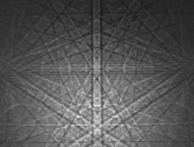
here you can see this (the middle band). Is this just an "eye illusion"? it seems that for any excess kikuchi line, forming one boundary of the band, with its darker parallel twin (the defecit kikuchi line) where is a DARK region, or DARK LINE just near to it, on other pictures it is a lot clearer and it seems that the kikuchi band is confined between to DARK DEFECIT LINES. IS IT? If so, what happened to the excess line?
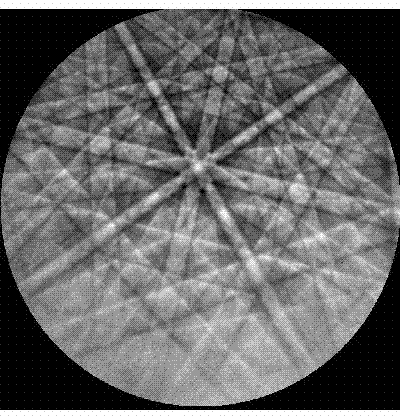
Another question: I understand that the band is 2theta(bragg) wide, but what happens in between I do not understand. What I understand is that the the in between the lines is just the diffused background of the scattering.
Anyone who can shed some light on the formation and origin of this contrast in the EBSD patterns from SEM, his contribution will be much appreciated. I have to prepare a little slide show and tell my colleagues at work about EBSD- which is something new we going to have here with our SEM soon, so I have to be "sort off" the expert. So to start with it can be nice to know these little details.
Thanks
Anton
anyone can point out to me how kikuchi bands are formed? And I mean bands, not lines. I finally managed to understand (I think) kikuchi lines: bragg diffraction is decreased in the incident direction (defecit=darker line) and enhanced in the "bragg" direction (excess=brighter line) and all this happens above the diffused background (backscattered electrons in all directions basically), which covers all the phosphor screen quite evenly throughout. And please correct me if I am wrong.
I did saw some TEM pictures where this phenomena can be seen. I also, however saw kikuchi bands: bright bands on a fairly dark background, confined between, what seems to me, 2 dark lines:
here you can see this (the middle band). Is this just an "eye illusion"? it seems that for any excess kikuchi line, forming one boundary of the band, with its darker parallel twin (the defecit kikuchi line) where is a DARK region, or DARK LINE just near to it, on other pictures it is a lot clearer and it seems that the kikuchi band is confined between to DARK DEFECIT LINES. IS IT? If so, what happened to the excess line?
Another question: I understand that the band is 2theta(bragg) wide, but what happens in between I do not understand. What I understand is that the the in between the lines is just the diffused background of the scattering.
Anyone who can shed some light on the formation and origin of this contrast in the EBSD patterns from SEM, his contribution will be much appreciated. I have to prepare a little slide show and tell my colleagues at work about EBSD- which is something new we going to have here with our SEM soon, so I have to be "sort off" the expert. So to start with it can be nice to know these little details.
Thanks
Anton