Solve Emitter Follower Circuit: Get Answers Now!

  • Thread starter JackB
  • Start date
In summary: V In summary, In Z = ΔVB/ΔIB So for the ΔIBIE = IB + ICIC = βIBΔIB = ΔIE/(β+1)Therefore ΔIB = RE(β+1)And the ΔVBΔVE = ΔVBΔVE = RE ΔIEΔVB = RE ΔIETherefore ΔVB/ΔIB = (β+1) RESo the input Z of the base would be around 300kohms without the two RB resistors? And the actual input Z (ignoring the 5k6 source?) would become
  • #1
JackB
3
1
Hi, I'm currently self learning electronics and am stuck on the emitter follower..
I'm wondering if I can talk it through with someone..?

In regards to In Z and out Z, running through a document I have..
In Z = ΔVB/ΔIB
So for the ΔIB
IE = IB + IC
IC = βIB
ΔIB = ΔIE/(β+1)

Therefore ΔIB = RE(β+1)


And the ΔVB
ΔVE = ΔVB
ΔVE = RE ΔIE
ΔVB = RE ΔIE

Therefore ΔVB/ΔIB = (β+1) RE


So the input Z of the base would be around 300kohms without the two RB resistors?
And the actual input Z (ignoring the 5k6 source?) would become 300k || 100k || 130k = 48k ohms

And in regards to outZ..
= (Vin - Vout)/output current
= (Vin - ΔVB)/ΔIE
Vin = Rsource ΔIB + RE ΔIE
Vin = Rsource ΔIE/(β+1) + RE ΔIE
Vin = [Rsource /(β+1) + RE] ΔIE
Zout = Rsource /(β+1)
Rsource/(β+1)

So in my case here it would be

100k || 130k || 300k || 5k6 || 3k3 = 5K / 100 = 50ohms

Am on the right lines so far?
Any help really appreciated
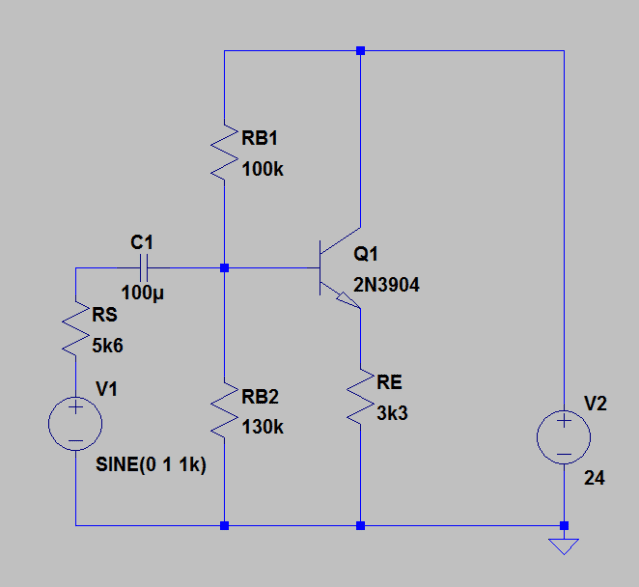
2822ec6.jpg
 
Engineering news on Phys.org
  • #2
JackB said:
And the actual input Z (ignoring the 5k6 source?) would become 300k || 100k || 130k = 48k ohms

That's correct.
JackB said:
Zout = 100k || 130k || 300k || 5k6 || 3k3 = 5K / 100 = 50ohms

That's wrong:

Ignoring C1 ( you can do so by high frequency ) it will be:

Zout = ( ( 100k || 130k || 5k6 ) / (1+β) ) || 3k3 = 50Ω

Well, same result, but in principle . . .
 
  • #3
Thanks! Ah yes I did the sum & posted it & then realized I'd forgot about the load so popped it in without thinking..

I'm also looking at Darlingtons in this configuration.. I assume the Zin & Zout would be calculated exactly the same way? Presumably the main difference would be higher β and so they'd have a lower output Z all else equal.

With regards to bootstrapping however I'm a little lost with Zin..
For output Z, I guess it's exactly the same as previous? All else equal, slightly higher perhaps as the source isn't as loaded as before.

However I'm unsure how to calculate the amplification.. So I'm stuck on input Z..
Mostly in my books it either says a little less than 1 or imagine it's 0.985 etc..
 
  • #4
Don't care about an amplification ≈ 0,99. A problem using darlington could be the amplitude of the voltage output ( rail to rail proporties ) in an output-stage. You could consider using a quasi-complimentary output-stage instead of a complimentary.
 
  • #5
The negative part of the signal being clipped as voltage increases?

Yes.. that's another thing I'm not 100% sure of in this circuit..

Why does this happen?

The positive can swing to within a saturation drop of V+.. so that is 0.1V - 0.3V ?
Then it can only turn off.. so that would take it to +6V + 0.6V ? So a maximum of 17.3Vpp *0.3535 = 6.1Vrms = 17.93dBu ? That seems too high.. Have I gone wrong somewhere?

Perhaps because it's asymmetrical? In this instance before clipping it would only be 10.8Vpp? *0.3535= 3.82Vrms = 13.86dBu ?
 
  • #6
As for the voltage gain.

Av = V1/VB * VE/VB where

V1 - input voltage
VB - voltage at base
VE - voltage at emitter

Av = Rin/(Rs + Rin) * RE/(re + RE) = 48kΩ/( 5.6kΩ + 48k) * 1kΩ/(1k + 0.007kΩ) ≈ 0.889V/V

Also Rin = RB1||RB2||( (β+1)*(RE + re) )

Where :
Rs - source internal resistance = 5.6kΩ
RE - emitter resistance = 1kΩ
re - small signal resistance between base and emitter looking into the emitter re = Vt/Ie ≈ 26mV/Ie = 26mV/3.7mA = 7Ω
https://www.physicsforums.com/threads/emitter-follower-help.631243/page-3#post-4061388

As for the output swing.
The voltage at transistor base cannot be larger than Vcc. And cannot be lower than 0.6V. So the max negative output voltage swing is equal to -Vmax = Ieq * RE||RL
 
Last edited:

FAQ: Solve Emitter Follower Circuit: Get Answers Now!

1.

What is an emitter follower circuit?

An emitter follower circuit is a type of transistor circuit that has the output voltage at the emitter terminal following the input voltage at the base terminal. It is commonly used as a buffer or voltage regulator.

2.

What are the advantages of using an emitter follower circuit?

Some advantages of using an emitter follower circuit include high input impedance, low output impedance, and low distortion. It also provides voltage gain and can be used as a buffer to isolate different parts of a circuit.

3.

How do you solve an emitter follower circuit?

To solve an emitter follower circuit, you can use Kirchhoff's laws and Ohm's law to determine the voltage and current values at each point in the circuit. You can also use the transistor's characteristics, such as the beta value and voltage drop, to calculate the output voltage.

4.

What are some common applications of emitter follower circuits?

Emitter follower circuits are commonly used in audio amplifiers, voltage regulators, and as output stages in power supplies. They can also be used as impedance matching circuits or as buffers in signal processing circuits.

5.

What are some challenges when working with emitter follower circuits?

One challenge when working with emitter follower circuits is thermal runaway, where the transistor can overheat and cause changes in performance. Another challenge is the limited voltage swing at the output, which can be improved by using a complementary emitter follower circuit.

Back
Top